For this question, there is no standard answer. The choice of which process to use depends on various factors such as the product, the company, and other considerations. This article will focus on what a lead frame is and compare two processes, with the aim of providing some useful insights.
What are lead frames?
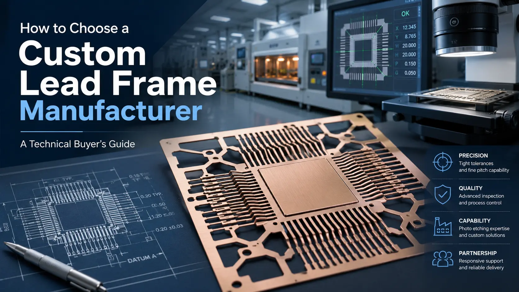
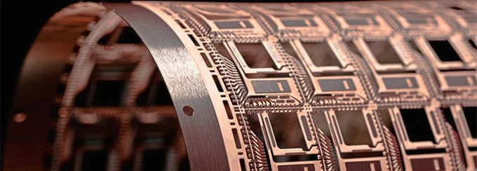
Lead frames are a fundamental component widely used in semiconductor devices, electronic components, and circuit boards. They serve as a structural framework for mounting and connecting integrated circuits (ICs) to the external environment. Lead frames are typically made from metals like copper, copper alloys, or aluminum, offering good thermal and electrical conductivity.
The design of lead frames is intricate and constantly evolving to meet the demands of modern electronics. They often consist of a complex arrangement of leads, tabs, and other structures that provide support and facilitate electrical connections. The evolving specifications of lead frames reflect the advancements in semiconductor technology, allowing for smaller, more efficient, and more reliable electronic devices.
Lead frames are key to ensuring the functionality and durability of a wide range of electronic products, from consumer electronics to automotive systems and industrial applications.
Advantages of Photo Etching vs. Stamping
photochemical etching
Photolithography offers a range of advantages when it comes to customizing lead frames, making it a popular choice in semiconductor manufacturing and electronic design. Here’s a breakdown of the key benefits:
1. No Mold Costs: Photolithography eliminates the need for expensive molds, reducing initial investment and ongoing production costs. This makes it an attractive option for smaller production runs and prototyping.
2. High Efficiency: The photolithography process is known for its speed and efficiency, allowing for rapid production cycles. This results in quicker turnaround times, helping companies bring products to market faster.
3. Low Expansion Rate Design: With photolithography, the precision of the design is maintained with minimal material expansion or deformation. This is critical in high-performance electronic applications where stability and reliability are essential.
4. Economic Optimization: The flexibility of photolithography allows for efficient design changes without incurring significant additional costs. This adaptability is invaluable in industries that require constant innovation and updates.
5. Low-Risk Entry Strategy: Given the lower initial investment and the flexibility of design, photolithography provides a lower-risk strategy for entering new markets or experimenting with new product lines.
6. Easy Product Design Updates: Changes to lead frame designs can be made quickly and easily, allowing manufacturers to adapt to evolving technology trends or customer requirements without significant retooling.
7. Precise Tolerances and Finer Details: Photolithography allows for extremely precise tolerances and the creation of intricate design details. This level of accuracy is crucial for modern electronics that require high performance and reliability.
8. No Scratches and Burrs: The process minimizes the risk of scratches and burrs, which are common issues with traditional manufacturing methods. This results in higher-quality lead frames with reduced risk of defects or failures.
The use of photolithography to customize lead frames offers a range of benefits, including cost savings, flexibility, efficiency, and precision, making it an ideal choice for modern electronic manufacturing.
Note: TMN has extensive experience in the custom lead frame industry and has more than ten years of experience in photochemical etching services.
Stamping
Stamping is a popular method for customizing lead frames, offering several key advantages, especially for large-scale manufacturing. Here’s why stamping is a preferred choice for producing lead frames in many industries:
1. Automation: Stamping is highly automated, allowing for consistent production with minimal human intervention. This automation enhances reliability and repeatability, ensuring each lead frame meets stringent quality standards.
2. High Speed: Stamping machines are designed for speed, allowing for rapid production cycles. This high-speed capability makes stamping ideal for large-scale manufacturing, reducing lead times and improving production efficiency.
3. Cost-Efficiency for Large-Scale Production: When it comes to high-volume manufacturing, stamping is a cost-effective method. The setup costs, including molds and dies, are offset by the low per-unit cost when producing in bulk, making stamping an economical choice for mass production.
4. Precision and Consistency: Despite its speed, stamping offers a high level of precision and consistency. The use of specialized dies ensures that each lead frame is produced with exact dimensions and minimal variation, which is critical for maintaining quality in electronic components.
5. Versatility in Design: Stamping can accommodate a wide range of designs, making it versatile for different applications. Manufacturers can create intricate patterns and complex shapes to meet specific requirements, providing flexibility in lead frame design.
6. Reduced Material Waste: Stamping is an efficient process that minimizes material waste, which can lead to additional cost savings and environmental benefits. This efficiency contributes to the overall cost-effectiveness of stamping.
7. Compatibility with Various Materials: Stamping is compatible with a range of materials commonly used for lead frames, including copper, copper alloys, and aluminum. This compatibility allows manufacturers to choose the best material for their specific application.
Overall, using stamping to customize lead frames offers significant advantages in terms of automation, high-speed production, cost-efficiency, and versatility. These benefits make stamping an excellent choice for manufacturers looking to produce large quantities of high-quality lead frames at a competitive cost.
Summarize:
If you’re focusing on complex designs or flexibility, photochemical etching tends to be more cost-effective. Although not mentioned earlier, it also performs better in terms of precision, reduced material waste, and material compatibility. However, if your priority is the cost per unit, stamping might be the more cost-effective choice.
Finally, if you’re interested in photochemical etching and want to learn more, feel free to contact us. As a professional photochemical etching manufacturer, we can offer you expert lead frame etching services tailored to your specific needs.WeChat and WhatsApp at +8613603056883; for inquiries, please email lydia.sales1@tmnetch.com;
Related articles:
Copper Etching: Reasons for using photo etching for copper metal