Photo etching is a technology that has been used for decades to etch metal parts for various applications. It is a process well suited for fabricating small, intricate parts with high accuracy. The photo etching process uses a light-sensitive material to mask the metal areas. The masked metal is then placed in an etching solution, which etches away the exposed metal.
What is photo chemical etching?
Photo chemical etching, also known as chemical milling or photo etching, is a process that uses chemicals to remove metal from a workpiece. This process is regularly used to create intricate parts with high accuracy. During the photochemical etching process, a negative film is placed over the metal workpiece. The film is then exposed to light, which creates a pattern of the desired design. The exposed areas of the film are then developed, which creates openings in the plate. The metal workpiece is then placed in an etching solution, which removes metal from the exposed areas. The etching solution typically comprises chemicals such as acids or bases. The etch depth can be controlled when the workpiece is left in the solution. After the etching process, the metal workpiece is typically rinsed with water to remove the etching solution. The workpiece is then dried, and the negative film is removed. The final product is a metal workpiece with the desired design. Photo chemical etching is a process that can be used to create a variety of metal parts with a high degree of accuracy. This process is often used to create intricate parts that would be difficult to produce using other methods.
Why is it used?
The photochemical etching process is used in a variety of industries for a variety of reasons. It is sometimes used because it is a more efficient way to produce a given product. In other cases, it is used because it is the only way to produce a product. The photochemical etching process is used in the electronics industry to produce printed circuit boards (PCBs). Printed circuit boards are the platform upon which electronic components are mounted. They are used in vehicles, electronic devices, including computers, cell phones, and televisions. The photochemical etching process is used to produce PCBs because it is a more efficient way to produce them than other methods, such as milling. The photochemical etching process is also used in the medical industry. It is sometimes used to produce implants, such as artificial hip joints. In other cases, it is used to produce stents, devices inserted into arteries to prop them open. The photo-chemical etching process is used to produce implants and stents because it is the only way to produce them with the required level of precision. The photochemical etching process has a wide range of applications because it is a more efficient way to produce many types of products. It is also the only way to produce some types of products.
Photo tool Design / CAD Design
The design of a photo tool is key to the success of the photochemical etching process. The designer must consider the size, shape and depth of the features to be etched and the type of material being etched. The design must also be compatible with the photomask and chemical processes. A few different methods can be used to create the photo tool. The first is to use a vector-based computer-aided design (CAD) program, such as AutoCAD. This method is best suited for simple designs with limited features. A raster-based CAD program, such as Photoshop, can be used for more complex designs. This method allows for more complex shapes and depths to be achieved. Once the design is complete, it must be transferred to the photo. This can be done using various methods, such as laser engraving, milling or photoresist. Each method has advantages and disadvantages, so choosing the best method for a particular design is important. After the design is transferred to the photo, it is ready for use in the photochemical etching process. This process involves exposing the photo to UV light, which activates the photoresist. The photoresist is then developed, which removes the exposed areas. The remaining photoresist protects the areas that are to be etched. The photo tool is then placed in the etching solution, which etches away the exposed metal. The photoresist is removed, leaving the desired features etched into the metal. The photochemical etching process is a versatile and accurate way to create complex shapes and features in metal. By carefully designing the photo tool, it is possible to achieve almost any desired shape or feature.
Metal Selection and Preparation for Photo Etching on Metal
Preparation is key when working with photo etching on metal. This process uses chemicals and light to etch patterns into metal, so it is important to understand which metals can be used and how to prepare them properly. There are many different types of metal that can be used for photo etching, but some are more difficult to work with than others. Copper, brass, and stainless steel are common choices, but each metal has quirks. For example, copper is easy to etch but can be difficult to clean, while brass is harder to etch but doesn’t require as much prep work. It is important to clean the metal surface before beginning the photo-etching process. This ensures that the chemicals will etch evenly and that the light can penetrate the metal. If the metal is clean or uneven, the results will be predictable. Once the metal is clean, it must be coated with a light-sensitive material. This can be a liquid or a film, and it determines how the light will react with the metal. A film coating is often used for more delicate work, while a liquid coating is more common for industrial applications. After the metal is coated, it is exposed to light. This step determines the depth of the etch and the overall shape of the final product. The light activates the photo-sensitive material, and the longer the metal is exposed, the deeper the etch. Once the desired depth is achieved, the metal is placed in a developing solution. This step removes the un-etched material, revealing the final product. The metal is then rinsed and dried, and the photo-etching process is complete.
UV Exposure and Development
The photochemical etching process involves UV light to expose and develop the desired image. This process is often used to create images on metal or other materials that are difficult to etch using traditional methods. The first step in the photo chemical etching process is to create a mask with the desired image. This mask is then placed over the material that will be etched. The material is then exposed to UV light, which causes the exposed areas to react with the material. After the material is exposed to UV light, it is placed in a developer solution. This solution removes the material not exposed to UV light, leaving behind the desired image.
Chemical Etching
Chemical etching is a process that uses chemicals to remove material from a substrate. This process can be used to create intricate designs and is often used to create circuit boards and other electronics. The process of chemical etching begins with a stencil. The stencil is placed on the substrate, and the desired design is cut into the stencil. Next, the substrate is placed in a chemical etching solution. This solution will remove the material from the substrate that is not protected by the stencil. Once the etching is complete, the stencil is removed, and the substrate is rinsed. The final step is to clean the substrate to remove any residue from the chemical etching process. Chemical etching is a very precise process that can create very intricate designs. This process is often used to create circuit boards and other electronics.
Photoresist Stripping
The photoresist stripping process is a critical step in the photochemical etching process. The etched metal will only have the desired finish or meet the required dimensional tolerances with proper stripping. There are two main types of strippers: wet and dry. Wet strippers are typically used for removing photoresist from stainless steel, copper, brass, and aluminum. They are typically more effective than dry strippers and produce less hazardous waste. The most commonly used wet strippers are based on hydrofluoric or hydrochloric acid. Dry strippers are typically used for removing photoresists from printed circuit boards (PCBs). They are typically less effective than wet strippers and produce more hazardous waste. The most commonly used dry strippers are based on hydrogen peroxide or hydroxide. The photoresist stripping process begins with the cleaning of the metal surface. The metal surface must be free of contaminants such as oils, fingerprints, dust, and flux residue. The next step is to apply the stripper. The stripper can be applied with a brush, a spray, or by dipping the metal into the stripper. After the stripper has been applied, it must be allowed to dwell on the metal surface for the recommended time. This time will vary depending on the type of stripper being used. After the recommended dwell time has elapsed, the metal must be rinsed with water to remove the stripper and any residual photoresist. The final step in the photoresist stripping process is to dry the metal surface. This can be done with a cloth, a compressed air duster, or by baking the metal in an oven.
Though the photochemical etching process was developed over thirty years ago, it is still widely used in various industries including aerospace, electronics, and medical device manufacturing. The process is advantageous over other etching methods because it is less expensive and allows for more precise control over the final product. Photo chemical etching is a versatile and reliable technology that will continue to be used in the future.
Final Inspection Quality Check
After the photo chemical etching process is completed, it is essential that a final inspection quality check is carried out. This will ensure that the product meets the required standards and specifications. There are a number of factors that need to be considered during a final inspection quality check. These include:
-The dimensions of the product -The tolerances of the product
-The appearance of the product
-The function of the product It is important to check all of these factors as they all contribute to the overall quality of the product. Dimensions are usually checked using calipers, micrometers or a ruler. Tolerances are the acceptable limits for the dimensions of the product. The appearance of the product is also important, as this can affect the function of the product. Functionality is usually checked by testing the product. This can be done in a number of ways, depending on the product. For example, electrical products can be tested using a multimeter, while mechanical products can be tested by using them in the intended application. Once all of these factors have been checked, the product can be deemed to be of acceptable quality.
What are the benefits of photochemical etching?
The photochemical etching process provides many benefits for manufacturers, especially in the electronics industry. This process can be used to create very detailed and intricate patterns on a variety of materials, including metals, plastics, and composites. etched components can have very tight tolerances and can be made with a high degree of accuracy. This process is also very versatile, as it can be used to create a wide variety of shapes and sizes. One of the biggest benefits of the photochemical etching process is that it is very cost-effective. This is because it is a relatively simple process that does not require a lot of expensive equipment. Additionally, there is no need for highly skilled labor, which keeps costs down. The process is also very fast, which reduces manufacturing time and further reduces costs. Another benefit of the photochemical etching process is that it is very environmentally friendly. The process does not generate any hazardous waste, and the chemicals used in the process are not harmful to the environment. Additionally, the process does not produce any harmful emissions. The photochemical etching process has a wide variety of applications. It is commonly used in the electronics industry to create printed circuit boards and various other electronics components. The process can also be used to create automotive parts, medical devices, and a variety of other industrial components. Due to its versatility, the photochemical etching process is an important tool for manufacturers across a wide range of industries.
What are the challenges of photochemical etching?
The photochemical etching process is a highly precise manufacturing method that can be used to create a variety of metal parts with extremely detailed designs. However, there are a few challenges that can arise when using this method. One challenge that can occur is etch creep. This is when the metal etchant solution starts to seep under the photoresist, which can cause the etching to become less precise. To prevent this, manufacturers need to use high-quality photoresist and ensure that it is properly applied to the metal. Another potential challenge is metal contamination. This can happen if the metal is not properly cleaned before the etching process, which can cause the etchant to not work as well and the final product to be less than perfect. To avoid this, manufacturers need to take care to clean the metal surface thoroughly before beginning the etching process. Despite these challenges, photochemical etching is still an extremely popular manufacturing method due to its high precision and ability to create detailed designs. By taking care to properly apply the photoresist and clean the metal surface, manufacturers can overcome the challenges of this process and create high-quality metal parts.
How can these challenges be overcome?
The Photo Chemical Etching Process can be challenged in a few ways. The first is ensuring all materials are correctly inputted into the process. This can be done by either having someone experienced in the etching process to do it or by following a set of instructions very carefully. The second challenge is making sure that the chemicals are correctly mixed. This can be done by following the instructions with the chemicals or consulting with someone experienced in the process. The last challenge is making sure that the etching process is done correctly. This can be done by either having someone experienced in the etching process do it or by following a set of instructions very carefully.
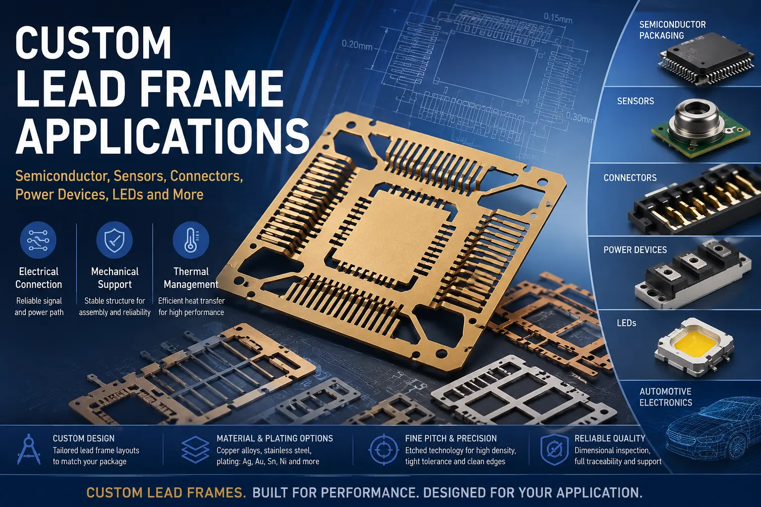
What are the applications of photochemical etching?
Photochemical etching is a process that can be used to create intricate and detailed patterns on various materials. It is often used in manufacturing electronic components, as it allows for very tight tolerances and precise patterns. It can also be used on various other materials, including metals, plastics, and glass. The photochemical etching process involves using light to etch a pattern into a material. A mask is placed over the material, and then light is shone through the mask. The light activates a chemical reaction in the exposed areas of the material, which causes the material to be etched away. The etched areas can be very small and can be controlled very precisely. The benefits of photochemical etching include that it is a very precise process, can be used to create very small features, and is a relatively low-cost process. It can also be used on a variety of different materials.
Best Solution | Inquiry Now
There are many obstacles for businesses that could limit production time, cost, budget and manpower effectively. One excellent manufacturing service that addresses such concerns effectively is photo chemical etching – at TMN Etch; we take great pride in offering innovative solutions tailored specifically towards these areas of importance.
Photochemical etching offers many advantages over traditional manufacturing methods, including the speed and accuracy of producing custom thin metal parts quickly and cost-effectively without needing an army of engineers and designers to do it for them. Due to this feature, photochemical etching has quickly gained widespread acceptance due to its efficiency and precision.
TMN Etch is your premier destination for developing an in-depth knowledge of chemical etching. With years of experience in this field, our specialists specialize in precise metal etching services to fit a range of thicknesses – providing maximum flexibility when reaching desired dimensions.
If you are searching for special photo etching services or need parts fabricated through our innovative etching process, don’t hesitate to contact us. Reach us easily via phone, WeChat and WhatsApp by dialling +8613603056883; for inquiries, please email lydia.sales1@tmnetch.com; lydia.sales1@tmnetch.com
Experience artistry and precision with TMN Etch! Discover countless possibilities and how our chemical etching services can elevate your business. Reach out now!