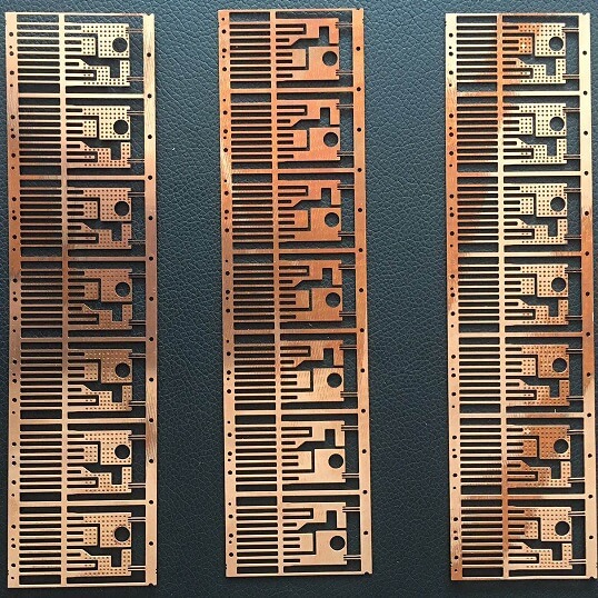
Custom micro lead frame
TMN's lead frame solutions are perfect for the fast-moving electronics industry. We provide a cost-effective and efficient way to make precise lead frames needed for super-small connections and lots of pins. Our method beats traditional stamping hands down!
The semiconductor industry stands out as the most widely used field for lead frames. Lead frames are integral to the packaging and assembly of integrated circuits (ICs), which are fundamental components in a vast array of electronic devices across numerous sectors.
What is Micro Lead frame?
A micro lead frame is a highly precise, miniaturized component used primarily in the semiconductor and electronics industries. It serves as the structural and electrical interface for microchips, providing the pathways for electrical signals between the chip and the outside circuitry. Here's a breakdown of its key aspects:
Features of Micro Lead Frames:
- Material: Typically made from high-conductivity metals such as copper alloys, silver, or other conductive materials. These may also be coated with gold, palladium, or nickel to improve conductivity and protect against corrosion.
- Size: "Micro" implies extremely small dimensions, making these lead frames suitable for compact and high-density electronic devices like smartphones, wearables, and medical devices.
- Design: Highly intricate with precise etching or stamping techniques to accommodate the delicate and complex requirements of modern microchips.
- Functionality:
- Support: Provides mechanical stability for the microchip.
- Connectivity: Facilitates electrical connections between the integrated circuit (IC) and external components through bonding wires or soldering.
- Thermal Management: Helps dissipate heat generated by the chip.
Manufacturing Techniques:
- Chemical Etching: Preferred for intricate designs due to its precision and capability to create fine, consistent patterns.
- Stamping: High-speed production for simpler designs.
- Laser Processing: Used for advanced applications requiring ultra-fine features.
Applications:
- Semiconductor devices (e.g., transistors, diodes)
- LEDs
- Microcontrollers
- Sensors
- High-frequency devices like RF chips.
The demand for micro lead frames is growing as devices become smaller, more powerful, and more integrated, requiring high-precision interconnect solutions. TMN provide all solutions for custom micro lead frames.
More About Lead Frames
What are the Properties of Lead Frame Material?
Lead frame materials must possess specific properties to meet the demands of semiconductor packaging:
High Electrical Conductivity: This ensures efficient electrical connections and minimal resistance within the IC package.
Good Thermal Conductivity: Effective heat dissipation is crucial for maintaining the operational temperature of the semiconductor die.
Mechanical Strength and Durability: Lead frames must withstand the stresses of manufacturing processes like wire bonding, molding, and soldering.
Corrosion Resistance: The material must resist corrosion to ensure long-term reliability.
Dimensional Stability: Lead frames must maintain their shape and alignment throughout the manufacturing process and during the IC's lifecycle.
Lead Frame Manufacturer: Partner for Custom Solutions
If you're seeking custom lead frames, look no further than TMN's, a leading manufacturer specializing in photochemical etching for lead frame production. We offer comprehensive, integrated solutions for all your lead frame needs, from design and prototyping to full-scale production.
With our advanced etching technology and extensive experience in the industry, we can create intricate lead frame patterns with high precision and accuracy. Our state-of-the-art equipment and skilled team ensure that every lead frame meets your specifications, whether for complex designs or high-volume production.
Our Team And Factory


Why Partner With TMN Etch
Get instant quote
