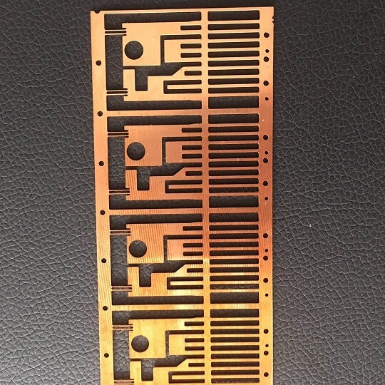
Custom brass lead frame
A brass lead frame is a type of lead frame made from brass, a copper-zinc alloy. It is commonly used in the electronics industry as a structural and electrical interface for semiconductor components, such as integrated circuits (ICs) and LEDs. Brass is chosen for its favorable mechanical and electrical properties, making it suitable for various applications.
· TMN has more than 10 years experience of OEM & ODM the shielding parts with 4000 square meters workshop and 100 experienced workers and engineers
· 5 automatic etching production lines with 20 meters long.
· 2 automatic cleaning equipment, 6 stamping machines.
· The production capacity of TMN is 300000pcs.
· Enough experience of export shielding parts to the USA, UK, Canada, Korea, Germany, Netherlands, Singapore, Russia, Iran, Israel, Austria, Australia and so on.
· Designed all Lead Frames for different industries, such as Aerospace, Automotive, Industrial, Marine, Medical, Military, Electronic, etc.
Key Features of Brass Lead Frames:
- Material Properties:
- High Conductivity: Brass offers good electrical conductivity, though it is slightly lower than pure copper.
- Corrosion Resistance: Brass resists corrosion and tarnishing, which enhances its durability.
- Workability: Brass is easy to stamp, etch, or machine into precise patterns required for lead frames.
- Thermal Conductivity: Provides adequate heat dissipation for electronic components.
- Surface Treatment:
- Brass lead frames are often plated with materials like nickel, gold, or silver to improve their conductivity, bondability, and resistance to oxidation.
- Plating also enhances solderability, making it easier to attach components during assembly.
- Manufacturing Techniques:
- Stamping: Used for high-volume production, creating lead frames quickly and efficiently.
- Etching: Allows for intricate designs and is ideal for smaller, more complex components.
- Applications:
- Semiconductor Devices: For connecting microchips to external circuits.
- LEDs: Brass lead frames are often used in light-emitting diodes.
- Power Electronics: Where mechanical strength and heat dissipation are critical.
- Consumer Electronics: For components in devices like smartphones and computers.
- Advantages:
- Cost-effective compared to other materials like pure copper.
- Good balance between strength, conductivity, and machinability.
Limitations:
- Brass is not as conductive as pure copper, which can limit its use in high-performance applications.
- May require additional surface treatments to meet certain performance standards.
Brass lead frames are widely used due to their affordability and suitability for many applications, particularly in consumer electronics and low-power devices.
FAQs about Custom Brass lead frame
1. What’s the production capacity of TMN for Lead Frame Parts?
· TMN has more than 10 years experience of OEM & ODM the shielding parts with 4000 square meters workshop and 100 experienced workers and engineers
· 5 automatic etching production lines with 20 meters long.
· 2 automatic cleaning equipment, 6 stamping machines.
· The production capacity of TMN is 300000pcs.
· Enough experience of export shielding parts to the USA, UK, Canada, Korea, Germany, Netherlands, Singapore, Russia, Iran, Israel, Austria, Australia and so on.
· Designed all Lead Frames for different industries, such as Aerospace, Automotive, Industrial, Marine, Medical, Military, Electronic, etc.
2. What are the main raw materials of Lead Frame covers and clips?
· Stainless Steel Alloys, Copper Alloys, Brass Alloys, Aluminum Alloys, Nickel Silver, Some other special requested metal materials.
3. What’s the thickness of the raw materials and the tolerance can be reached by photochemical etching?
· Thickness: 0.001 inch to 0.078 inch
· Tolerance : +/- 0.001inch
4. What’s the process for coating/plating after photo etching can be done?
· Nickel plating 1~10μ
· Tin plating 1~10μ
· Ag plating 1~10μ
· Au plating 1~10μ
5. What are the advantages of TMN manufacturing plants?
· Rapid for prototypes without any tools (1~3 days can be finished the prototypes)
· No scratches and no burrs
· Designs can be changed flexibly
· High precision with a small tolerance
6. What’s the lead time for samples, and how many samples can be provided for the first time?
· 10PCS samples can be provided for confirmation and 4 days as the lead time for common materials, if the raw material is special, it will take some days to prepare raw materials.
· For mass production, it is about 10 days after confirming all details.
7. If you want to inquiry TMN, What should you do?
Just need to send an email to lydia.sales1@tmnetch.com with drawings at the format of DXF, DWG, PDF, 7*24 hours available.
Our Team And Factory


Why Partner With TMN Etch
Get instant quote
