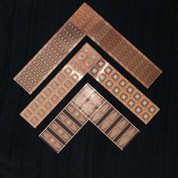
Custom C1100 C7025 lead frame
The production capacity of TMN for Lead Frame Parts
· TMN has more than 10 years experience of OEM & ODM the shielding parts with 4000 square meters workshop and 100 experienced workers and engineers
· 5 automatic etching production lines with 20 meters long.
· 2 automatic cleaning equipment, 6 stamping machines.
· The production capacity of TMN is 300000pcs.
· Enough experience of export shielding parts to the USA, UK, Canada, Korea, Germany, Netherlands, Singapore, Russia, Iran, Israel, Austria, Australia and so on.
· Designed all Lead Frames for different industries, such as Aerospace, Automotive, Industrial, Marine, Medical, Military, Electronic, etc.
FAQ about C1100 C7025 Lead frame
What are the main raw materials of Lead Frame covers and clips?
· Stainless Steel Alloys, Copper Alloys, Brass Alloys, Aluminum Alloys, Nickel Silver, Some other special requested metal materials.
What’s the thickness of the raw materials and the tolerance can be reached by photochemical etching?
· Thickness: 0.001 inch to 0.078 inch
· Tolerance : +/- 0.001inch
What’s the process for coating/plating after photo etching can be done?
· Nickel plating 1~10μ
· Tin plating 1~10μ
· Ag plating 1~10μ
· Au plating 1~10μ
What are the advantages of TMN manufacturing plants?
· Rapid for prototypes without any tools (1~3 days can be finished the prototypes)
· No scratches and no burrs
· Designs can be changed flexibly
· High precision with a small tolerance
What’s the lead time for samples, and how many samples can be provided for the first time?
· 10PCS samples can be provided for confirmation and 4 days as the lead time for common materials, if the raw material is special, it will take some days to prepare raw materials.
· For mass production, it is about 10 days after confirming all details.
If you want to inquiry TMN, What should you do?
Just need to send an email to lydia.sales1@tmnetch.com with drawings at the format of DXF, DWG, PDF, 7*24 hours available.
What is the Purpose of a Lead Frame?
The primary purpose of a lead frame is to support and connect the semiconductor die within an integrated circuit package. Lead frames serve several key functions:
Mechanical Support: They provide a stable structure to which the semiconductor die is attached, ensuring it stays in place during manufacturing and use.
Electrical Connections: Lead frames create the pathways for electrical connections between the semiconductor die and external circuits. These connections are typically made through bonding wires or soldering.
Heat Dissipation: The metal structure of lead frames helps dissipate heat generated by the semiconductor die, contributing to the thermal management of the IC package.
Protection: Lead frames often serve as a base for encapsulation, which protects the semiconductor die from environmental factors like moisture and physical damage.
What are the Properties of Lead Frame Material?
Lead frame materials must possess specific properties to meet the demands of semiconductor packaging:
High Electrical Conductivity: This ensures efficient electrical connections and minimal resistance within the IC package.
Good Thermal Conductivity: Effective heat dissipation is crucial for maintaining the operational temperature of the semiconductor die.
Mechanical Strength and Durability: Lead frames must withstand the stresses of manufacturing processes like wire bonding, molding, and soldering.
Corrosion Resistance: The material must resist corrosion to ensure long-term reliability.
Dimensional Stability: Lead frames must maintain their shape and alignment throughout the manufacturing process and during the IC's lifecycle.
What is Lead Frame Paddle Size?
The paddle is the central portion of the lead frame where the semiconductor die is attached. Paddle size varies depending on the size of the semiconductor die and the specific requirements of the IC package. It plays a crucial role in:
Die Attachment: The paddle must be large enough to securely attach the semiconductor die.
Heat Dissipation: A larger paddle can improve heat dissipation by providing more surface area.
Mechanical Support: The paddle's size contributes to the overall stability of the IC package.
Paddle size is often defined by the package type and the specific design requirements of the IC.
Our Team And Factory


Why Partner With TMN Etch
Key Client Partnerships


Get instant quote
