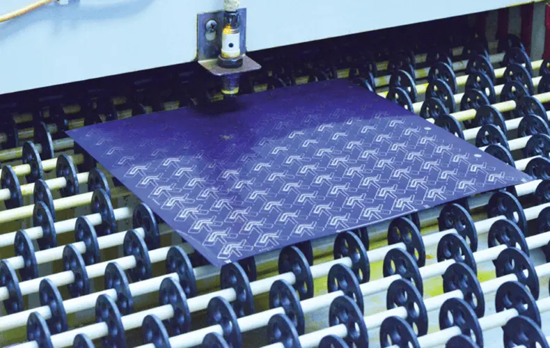
Photo chemical etching, also known as photochemical machining, is a manufacturing process, which involves producing metal parts using chemical processes. Although the process might sound unfamiliar to some, it is used widely by various manufacturing sectors to acquire consistent and accurate metal components by incorporating low costs. This process starts with printing the design prototype onto the photoresist to laminate onto the metal parts. The areas of the photoresist which does not have the printed design are then removed, and the printed design is etched using etchants.
Importance of photochemical etching
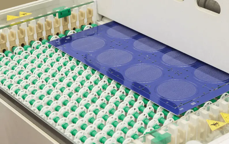
Chemical milling or photo chemical etching is a controlled method of manufacturing metals, and it is one of the reasons behind its growing popularity. Once the designs have been printed on the metal sheet, thermal controlled etchants such as ferric chloride derive the components. The acid works its way to the design while the rest of the metal, free of design, is protected by the photoresist.
The result is accurate and consistent, regardless of the complexity of the design. Even after the etching process is completed, the metal retains its former characteristics, which would not have been possible if the metal were laser cut or stamped. Even though it is least invasive, it ensures that the outcomes match your desired specifications.
Application of photochemical etching in communications and electronics
For a few years, photo chemical etching has been a vital part of the electronics manufacturing industry because it offers numerous perks. For starters, even if the complexity of the design varies, the cost of producing those does not increase, and as a result, designers can complete their targets successfully. Here are some of the areas in which chemical etching is applied in electronics and communication:
- EMI& RFI Shielding
The aim of the EMI shielding procedure is to control Electronic Magnetic emissions, and as of today, it is widely performed across diverse manufacturing sectors. It is majorly used in the electronics and telecommunications sector to avoid the interference caused by electromagnetic signals. This process for producing metal cans is necessary when dealing with problematic areas of a circuit or components emitting a high amount of radiation.
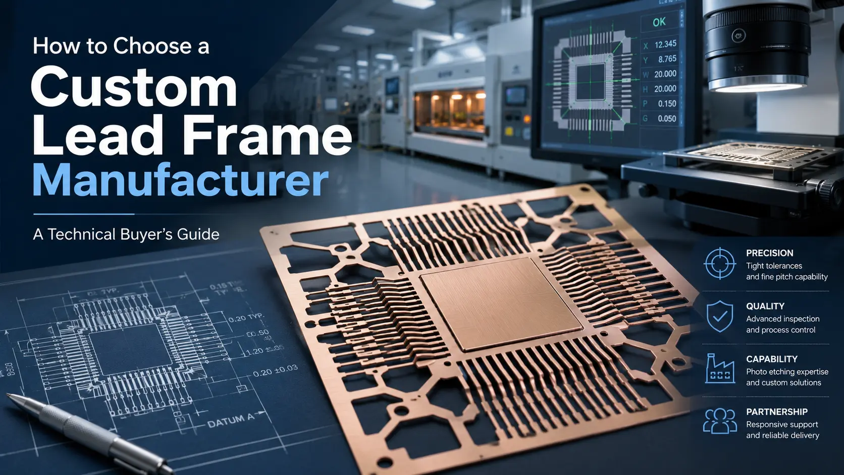
- Lead frames
Although semiconductors used in electronic appliances were manufactured by the stamping process over the years, they could not offer high preciseness and consistency. That is why designers have shifted towards photo chemical etching as it caters to the demand for smaller, thinner, and accurate assembly solutions. As a result of this, lead frames produced reduces the production lead time while featuring high tolerances.
- Shims & Washers & Spacers
Shims & Washers & Spacers are critical components of the communications manufacturing sector, but discrepancies were found in finishing such components earlier. However, with Photo chemical etching, stress-free and burr-free products can be produced while ensuring high precision. Some of the common types of shims, washers, and spacers manufactured with chemical mining are cylinder rings, pistons, fasteners, etc.
- Speaker grilles
Speaker grills, which were earlier produced by weaving aluminum wire, have certain limitations in performance. Nowadays, grilles are manufactured by following the photo chemical etchingmanufacturing process, and thus. As a result, the grilles are more durable but thinner. Designers are even producing finer designs like logos and other decorative features with etching.
- Mesh filters
Another critical component of the communications industry, mesh filters, are now produced by etching stainless steel by embracing the Photo chemical etching. To reduce clogging and ensure the desired throughput, mesh filters produced by etching can be fully customized.
Advantages of photochemical etching in communications and electronics
Now that you have understood the various applications of photo chemical etching in the communications and electronics industry, you should know its advantages. The etching process is super easy for designers, and there are no areas of errors because the designs are printed from a CAD machine and not done manually.
Even on the thinnest and delicate metal sheets, accuracy is maintained, regardless of the design’s complexity. Some metal parts are partly produced by etching, and designers can cater to such requirements without changing the design layouts. As a result, engineers manage to make bulk orders even while ensuring high precision.
TMN is one of the most reliable chemical etching companies that specialize in photochemical machining. To know about the type of etched metal components your company needs, check out what TMN has to offer.