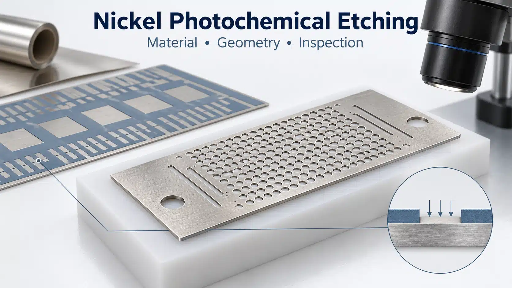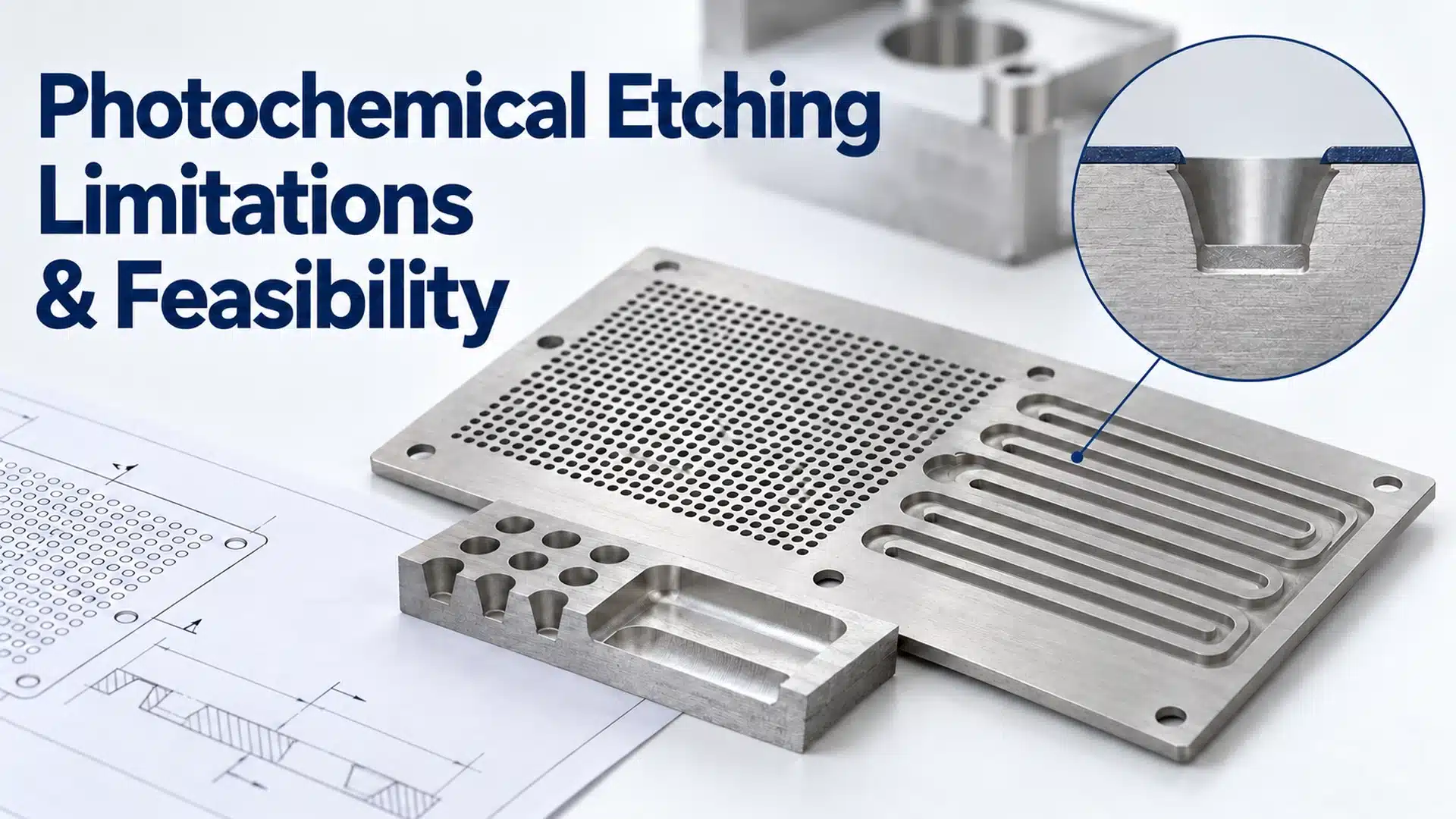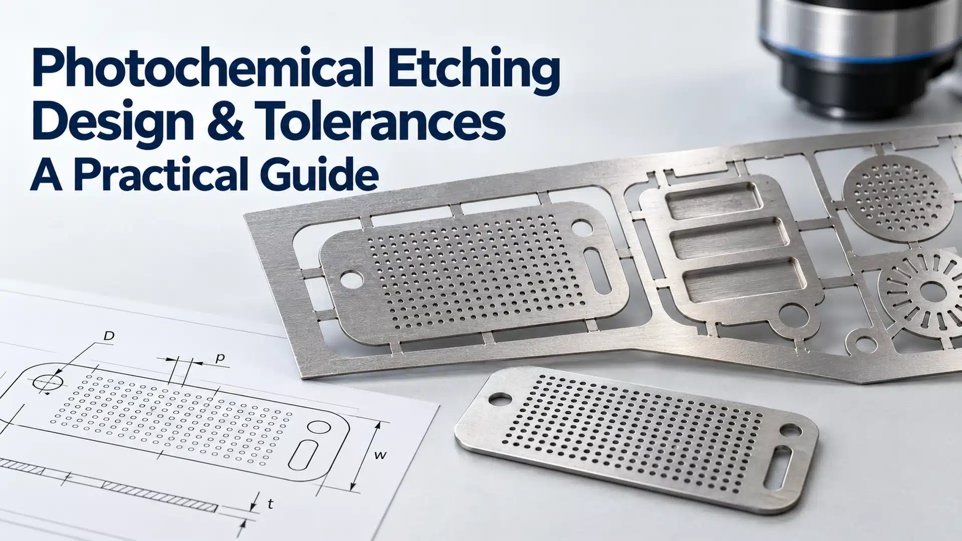

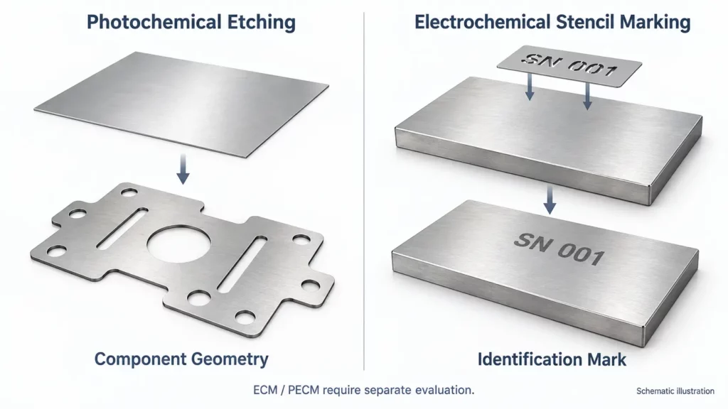
Chemical etching can manufacture thin metal parts from a drawing. Electrical etching, when used to mean electrochemical stencil marking, creates identification on an existing metal part. Choose by the required output, material, geometry, and acceptance criteria.
This guide compares photochemical etching for metal part manufacture with electrochemical stencil marking. The terms electrical etching and electrolytic etching can also describe broader electrochemical processes. Those uses, including electrochemical machining, need a separate assessment.
Start with a clear question: do you need a new functional component, a surface mark, or both?
Chemical Etching vs Electrical Etching: Quick Comparison
The two processes below usually address different tasks. Decide what must be delivered before comparing precision, speed, or price.
| Requirement | Photochemical etching for metal parts | Electrochemical stencil marking |
|---|---|---|
| Main output | A metal profile, opening, or controlled-depth feature | Text, a symbol, or identification on an existing part |
| Starting workpiece | Metal sheet or another suitable workpiece | An existing metal part requiring a mark |
| Pattern control | Photoresist pattern and chemical etchant | Stencil, electrolyte, and electrical settings |
| Main inspection | Dimensions, openings, depth, and edge condition | Mark position, legibility, surface condition, and required durability |
| Selection inputs | Drawing, alloy, thickness, features, and tolerances | Alloy, finish, mark content, location, and acceptance requirements |
| Production planning | Sheet layout, processing, separation, and inspection | Part loading, stencil changes, marking, cleaning, and inspection |
Here, electrical etching means the stencil-marking application. This table does not describe every form of electrolytic material removal.
If your task requires complex three-dimensional geometry, assess the relevant machining processes separately. A comparison with surface marking will not resolve that manufacturing decision.
What Are Chemical, Electrical, and Electrolytic Etching?
Chemical Etching and Photochemical Etching for Metal Parts
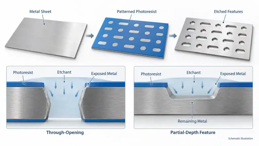
Chemical etching removes material through a chemical reaction. In photochemical etching, a light-sensitive coating called photoresist protects the metal that must remain. Imaging and developing expose the areas where an etchant, a chemical solution that removes metal, will act.
The process can create outside profiles, holes, slots, and suitable partial-depth features. A typical route includes cleaning, resist coating, exposure, developing, etching, and resist removal.
The design controls where removal occurs; the material and process conditions affect the final geometry. Our photo etching overview explains the manufacturing sequence.
Electrical Etching in This Comparison: Electrochemical Stencil Marking
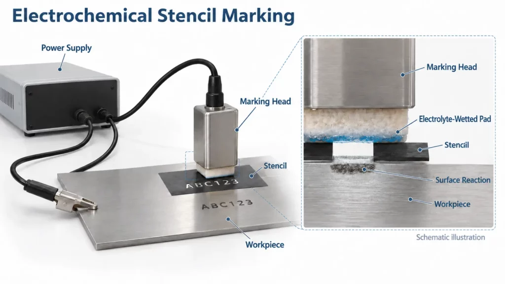
Electrochemical stencil marking uses a power supply, a suitable electrolyte, and a stencil that defines the image. The electrolyte carries current between the marking head and the workpiece through the stencil openings.
The resulting surface reaction creates the mark. Describing this as burning a logo into the metal gives the wrong explanation.
Equipment may offer alternating current (AC), direct current (DC), or combined operating modes. Mark appearance and material removal depend on the system, electrolyte, alloy, and settings.
Electrolytic Etching and Other Electrochemical Processes
Electrolytic etching is broader than stencil marking.
Electrochemical machining (ECM) can generate component geometry through controlled metal dissolution. Precision electrochemical machining (PECM) is a related approach used for precision machining applications, as described by EMAG.
A statement that electrical etching “only makes shallow marks” therefore needs a narrow scope. It does not describe the whole electrochemical manufacturing field.
Chemical Etching for Electronic and Electrical Components
Lead Frames, Contacts, and EMI/RFI Shields
Chemical etching for electronics concerns the manufacture of functional metal components. The fact that a part carries current or belongs in an electrical assembly does not make its manufacturing process electrical etching.
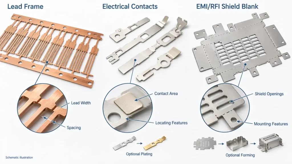
Examples include lead frames, suitable thin metal contacts, and EMI/RFI shielding components. EMI and RFI mean electromagnetic interference and radio-frequency interference.
For a lead frame, identify the lead widths, spacing, and registration features needed for assembly. For an etched electrical contact, define the contact area, slots, and features that locate the part. For a shielding component, review openings, mounting features, and any forming requirements.
Then separate critical dimensions from noncritical edges. Give tighter requirements to features that control fit or function, rather than applying the same tolerance to the entire drawing.
This makes chemically etched electrical components a distinct application topic. It should not be confused with putting a serial number on an already manufactured component.
Geometry Is Only One Part of Electrical Performance
A dimensionally correct part still needs to meet its functional requirements. Define those requirements before approving the manufacturing route.
For contacts, the project may require checks of contact resistance, contact force, or surface finish. A shielding assembly may need performance testing under its intended conditions. These checks are application-specific; they are not a universal test list for every etched component.
Also state the material grade, temper, and any plating requirements. Agree whether measurements apply before or after finishing and forming.
Chemical etching does not automatically improve conductivity or guarantee electrical reliability. If identification is also needed, define it as a separate requirement and identify any contact, seal, or bonding surfaces where marking is restricted.
How to Compare the Processes Against Your Requirements
Material, Thickness, and Surface Condition
Specify the actual alloy and thickness. “Stainless steel” or “copper” alone may leave important details unresolved.
For part manufacture, ask the supplier to assess the combination of material, thickness, openings, and remaining metal sections. For stencil marking, provide the alloy and final surface state so the marking supplier can select and test a suitable process.
A conductive base metal does not by itself confirm marking suitability. Coatings, oxidation, and other surface conditions may affect the process.
Use a sample in the intended final condition for approval. A successful test on unfinished stock does not establish the result after a different finishing sequence.
Geometry, Tolerances, and Etch Depth
Precision needs a defined measurement.
For a photo-etched part, that might be a hole size, slot width, feature position, or partial-etch depth. For a mark, it might be its location, image dimensions, contrast, or permitted surface change.
These are different acceptance conditions. Comparing them with one “high precision” label hides the actual requirement.
For thin parts, identify the smallest openings and narrow metal bridges between features. Ask how lateral etching, called undercut, is allowed for and how critical features will be measured. Review photochemical etching tolerances and limits before assigning a general tolerance.
Mark Legibility, Repeatability, and Inspection
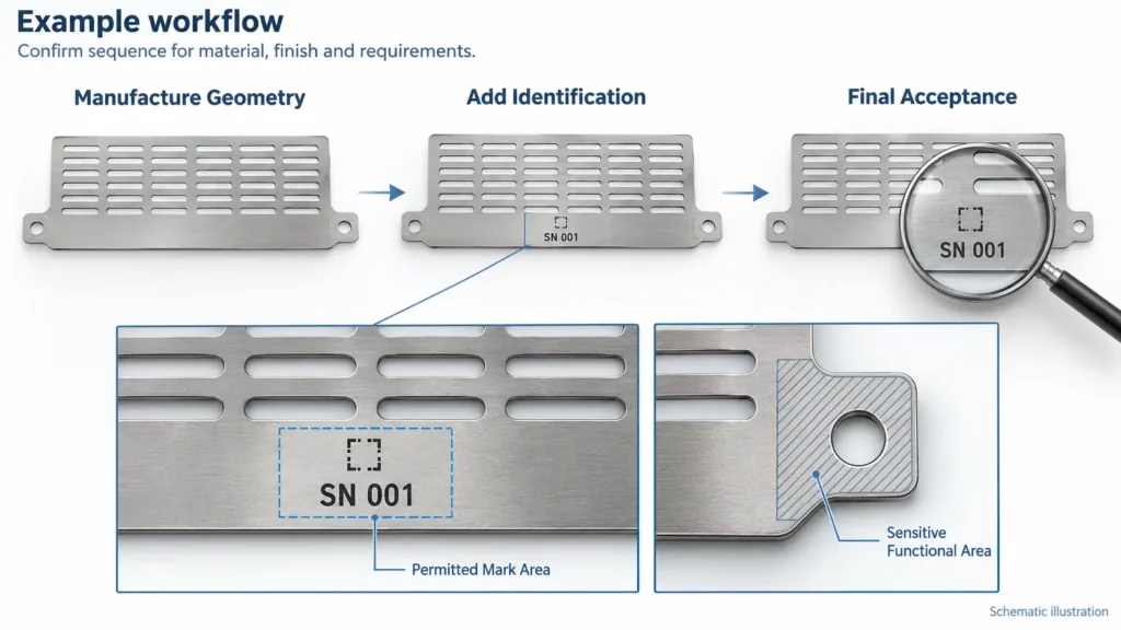
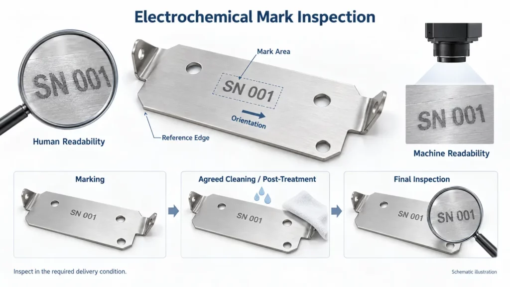
Define a passing mark before production. State the text or code, location, size, orientation, and required reading method.
If a machine must read the mark, agree on the reader and verification conditions. If the mark must remain readable after cleaning or service exposure, define those conditions and approve a representative sample.
Include post-mark cleaning in the process plan. Check the completed part rather than judging only the mark immediately after processing.
Production Volume and Automation
Neither process should be classified by batch size alone, so stencil marking is not limited to manual work.
Compare the complete workflow: preparation, loading, processing, cleaning, inspection, and rework. For part manufacture, also account for sheet layout, part separation, and downstream operations.
Ask for throughput based on the actual part mix and acceptance plan. A short reaction time is not the same as a short production cycle.
Cost, Equipment, and Waste Management
Compare Cost Within the Same Task and Acceptance Criteria
First decide what you are buying. A quote to manufacture a metal contact and a quote to mark an existing contact cover different outputs.
For alternatives within the same task, align the drawing, quantity, finish, inspection, packaging, and delivery scope. Then compare preparation, consumables, labor, finishing, rejects, and transport.
Use cost per accepted part or accepted mark, not equipment price alone. Our photochemical etching cost guide explains the factors to include in a manufacturing quotation.
In-House Production or Outsourcing
An in-house decision includes equipment, support systems, trained staff, maintenance, and utilization. An outsourcing decision includes supplier capability, sample approval, lead time, and delivered cost.
Evaluate these within the chosen task. A stencil-marking station and an industrial photochemical etching line require different operating plans.
Before committing to in-house manufacturing, review the chemical etching equipment and support systems the process needs.
Cleaning, Residues, and Waste Treatment
Plan chemical handling and waste treatment around the selected process. For marking, follow the equipment and electrolyte supplier’s post-process instructions; residual electrolyte can create a corrosion risk.
For manufacturing, include cleaning, rinsing, bath control, and waste treatment in the operating scope.
Neither process earns an automatic environmental advantage. Compare chemical use, waste composition, water, energy, yield, and treatment for the same required result.
Which Process Fits Your Project?
The following are selection examples, not reported customer projects.
You Need a Thin Metal Component
Suppose you need a thin contact or shielding blank with defined openings. Start with a photochemical etching drawing review.
Identify the functional features, material, thickness, and acceptance requirements. Confirm that the complete route, including any forming or finishing, can deliver the part.
You Need Identification on an Existing Metal Part
Suppose the part already exists and needs text or a serial number. Assess electrochemical stencil marking against the final surface and identification requirements.
Provide the mark location and approve a sample after the agreed cleaning and finishing sequence. Manufacturing a new profile is not the task being evaluated.
You Need Both a Manufactured Part and Identification
Treat geometry and identification as two linked requirements. Decide where the mark belongs and when it should be applied.
Approve both the component and its identification in the final delivery condition. If the main requirement is complex three-dimensional material removal, request a separate machining assessment, including ECM or PECM where relevant.
FAQs About Chemical, Electrical, and Electrolytic Etching
What Does “Electrical Chemical Etching” Mean?
The phrase needs context. It may be used for an electrically driven electrochemical process, or it may confuse that process with chemical etching for electrical components.
Specify whether you need component geometry or identification. Then ask the supplier to name the actual process and describe its scope.
Is Electrical Etching the Same as Electrolytic Etching?
The terms overlap in some contexts, but they do not identify one fixed application. Electrolytic etching can describe electrically driven material removal, while electrical etching is also used for stencil marking.
Confirm what the supplier means before applying a comparison of cost, accuracy, or capacity.
Can Electrical Etching Replace Photochemical Etching for Metal Parts?
The stencil-marking process compared here is not a substitute for manufacturing a thin component with through-features.
Other electrochemical processes, including ECM, can generate geometry. Their suitability must be assessed against the actual workpiece and drawing rather than inferred from the word “electrical.”
Can Chemical Etching Produce Electrical Contacts?
Yes, for suitable thin metal contact designs. Confirm the alloy, thickness, geometry, surface treatment, and required electrical or mechanical performance.
Approve dimensions and functional requirements separately. A finished outline alone does not establish contact performance.
Share Your Drawing and Acceptance Requirements
For a thin metal component, share your requirements with TMNetch’s chemical etching team:
- Drawing and critical dimensions;
- Material grade, temper, and thickness;
- Finish, forming, and inspection requirements;
- Quantity and delivery schedule;
- Any identification content, location, and final surface requirements.
A drawing review can establish whether photochemical etching fits the component and what needs confirmation before sampling or production.