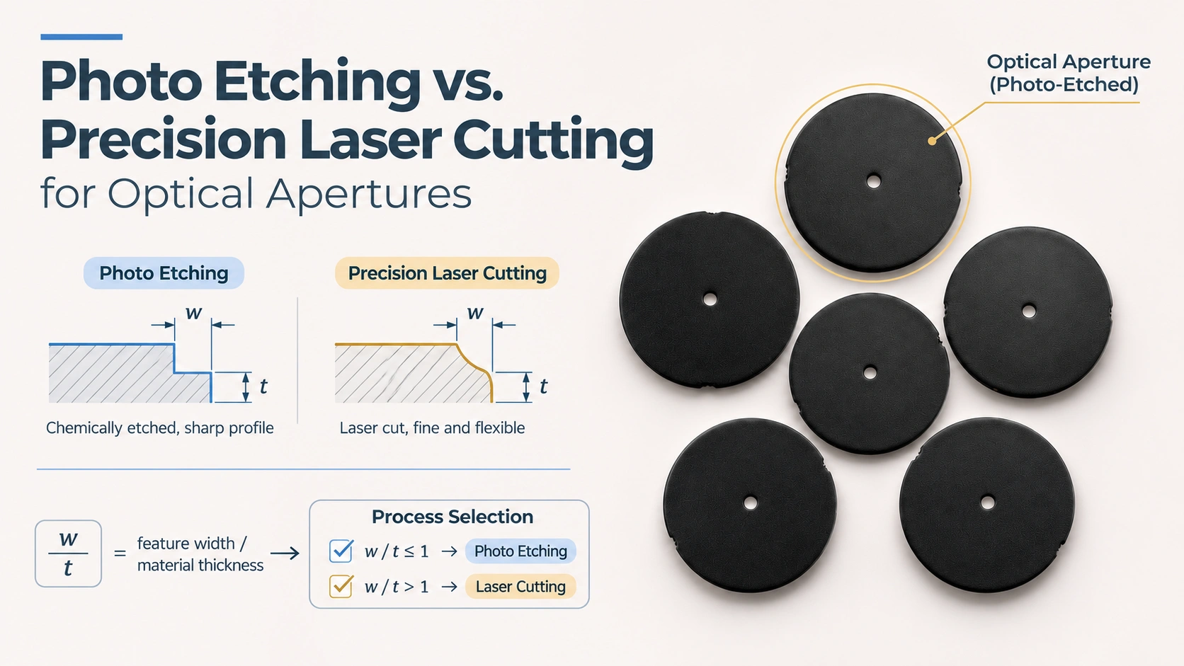

A custom optical aperture can present an interesting manufacturing problem. Most of its geometry may be well suited to photochemical etching, while a single narrow slit or critical edge requirement pushes the design beyond the process’s demonstrated capabilities.
Should the entire component be manufactured differently? Can the etched design be optimized without changing its optical function? Or would precision laser cutting provide a more suitable route?
These are important questions for engineers developing spectrometers, imaging systems, life science instruments, and other optical assemblies.
Photochemical etching is an excellent starting point for evaluating complex thin-metal optical components. However, the final manufacturing decision should depend on the functional opening, material thickness, dimensional tolerances, and edge requirements—not simply the preferred production technology.
At TMNetch, we approach optical aperture manufacturing with an etching-first strategy. When a critical requirement cannot be achieved reliably through etching, we evaluate precision laser cutting and adopt it when the alternative process can meet the approved specifications.
Key Takeaways
- Photochemical etching is particularly worth considering for thin-metal optical apertures with multiple openings, complex profiles, and integrated mounting features.
- Minimum opening size alone does not determine etching feasibility. Material thickness, functional tolerances, edge geometry, and production repeatability must also be evaluated.
- Precision laser cutting becomes an alternative when essential optical requirements fall outside the validated etching process window.
- Switching to laser cutting introduces additional considerations, including kerf geometry, thermal effects, and edge condition.
- A multi-process manufacturing approach allows engineers to retain the advantages of etching wherever possible and select another qualified process when necessary.
Why Photo Etching Should Be Evaluated First for Optical Apertures
The first manufacturing question is not whether a laser can cut the aperture. It is whether the required component can be produced effectively through photochemical etching.
For many thin-metal optical designs, the answer is worth investigating.
Complex Optical Features Can Be Manufactured Together
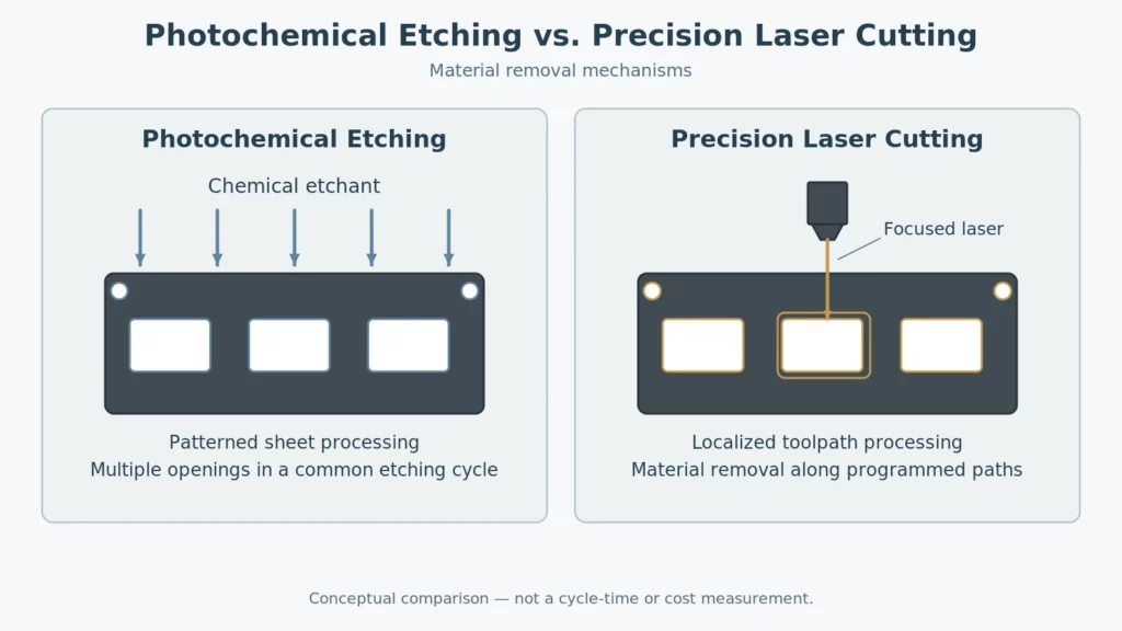
In photochemical machining, a patterned photoresist protects selected regions of a metal sheet while an etchant removes exposed material.
The pattern can define multiple features within the same component, including optical openings, locating holes, mounting slots, and external profiles.
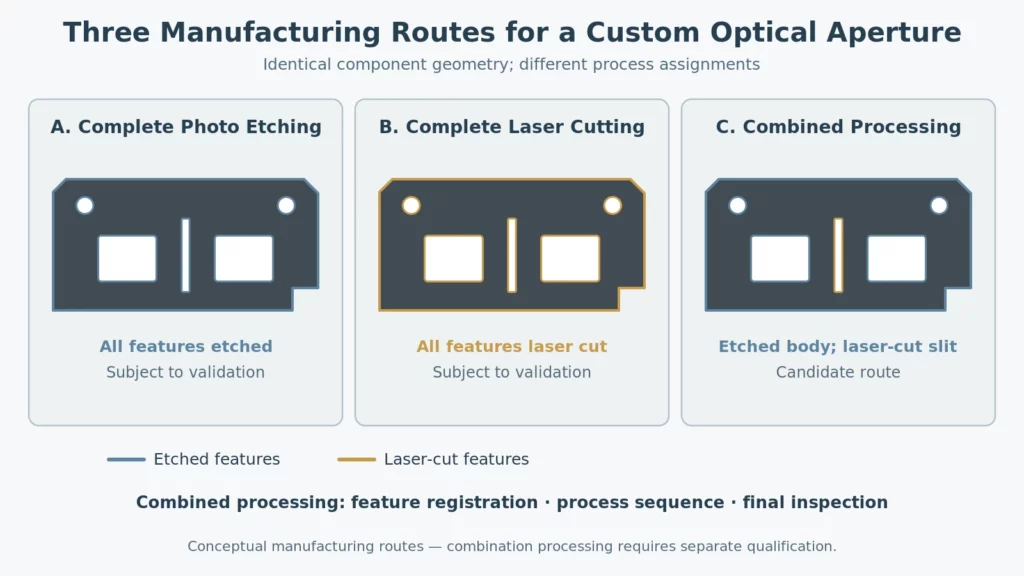
Consider a metal aperture plate with three rectangular windows, two locating holes, and an asymmetric outer contour. Rather than evaluating each feature as an isolated machining operation, engineers can assess the complete two-dimensional pattern as one etched design.
This is particularly valuable when the optical component combines several functional and mechanical features.
The same principle applies to aperture arrays and patterned light shields, where many openings must maintain defined dimensions and positions within a thin metal structure.
Etching Avoids Mechanical Cutting Loads and Localized Laser Heating
Chemical dissolution removes material without the mechanical shearing action of punching or the concentrated laser energy used in thermal cutting.
For delicate metal foils, this eliminates certain sources of cutting-induced burrs and localized thermal effects associated with other manufacturing methods.
That does not mean an etched component is automatically free from dimensional variation or deformation.
The original material condition, residual stress, lateral material removal, and part-handling method can still influence the finished geometry. These factors are part of the engineering considerations for photochemical machining.
The advantage is therefore not that etching eliminates every manufacturing risk. It is that the process avoids some mechanical and thermal cutting mechanisms while offering considerable flexibility in planar component geometry.
Panel-Based Manufacturing Supports Repeated Optical Patterns
Photochemical etching processes multiple features across a metal sheet within a common manufacturing cycle.
For an aperture array or a production panel containing several optical components, this means that numerous openings and profiles can be defined through the same patterned tooling.
By comparison, laser cutting generally removes material through localized machining along programmed paths.
The relative economics depend on sheet utilization, feature complexity, processing time, production quantity, and inspection requirements. Nevertheless, panel-based photo etching is particularly worth evaluating when a project involves complex patterns or large numbers of repeated openings.
These characteristics make etching a logical first candidate for suitable optical apertures rather than merely a lower-cost alternative to another process.
Define the Etching Process Window Before Selecting a Manufacturing Route
A common mistake in optical aperture manufacturing is to evaluate feasibility using a single supplier specification.
A published minimum hole diameter or general dimensional tolerance provides useful information, but it does not establish whether a particular optical component can be manufactured.
A more useful approach is to define the validated process window.
For this discussion, the etching process window is the combination of material, thickness, feature geometry, tolerances, and production conditions within which the required component can be manufactured and verified.
Opening Size and Material Thickness Must Be Evaluated Together
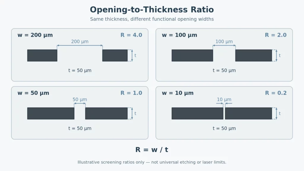
The relationship between aperture size and sheet thickness provides an initial manufacturability indicator.
A simple screening ratio is:
Opening-to-thickness ratio = w / t
Where:
- w is the required functional aperture width or diameter.
- t is the metal thickness.
Consider four hypothetical slit designs on the same 0.050 mm metal foil.
| Required slit width | Metal thickness | Opening-to-thickness ratio |
|---|---|---|
| 0.200 mm | 0.050 mm | 4.0 |
| 0.100 mm | 0.050 mm | 2.0 |
| 0.050 mm | 0.050 mm | 1.0 |
| 0.010 mm | 0.050 mm | 0.2 |
As the required opening becomes smaller relative to the thickness, the design requires closer evaluation of through-etching behavior, dimensional control, and the resulting aperture profile.
However, the ratio is not an acceptance criterion.
For example, one published chemical etching design guideline lists a standard minimum hole or slot dimension of 0.100 mm for material thicknesses between 0.010 mm and 0.100 mm.
This is a supplier-specific design reference, not a universal etching limit. Smaller features may be possible through specialized process development.
The important point is that changing the opening-to-thickness ratio changes the manufacturing problem. It does not independently determine which process will succeed.
Separate Feature Feasibility From Production Capability
Producing an aperture and producing it repeatedly within a specified tolerance are different engineering tasks.
A manufacturing review should distinguish three levels of evidence.
| Evaluation level | Question to answer |
|---|---|
| Feature feasibility | Can the required opening be formed? |
| Sample conformity | Does the manufactured sample meet the drawing? |
| Production capability | Can the process maintain the requirement across the intended production quantity? |
For optical components, the distinction becomes especially important when a critical feature has a narrow tolerance band.
A successful prototype demonstrates that a particular sample can meet the requirement. It does not, by itself, establish the variability of subsequent production.
A meaningful process capability evaluation compares the variation of a stable manufacturing process with the specified tolerance limits.
Where statistical capability is required, sufficient representative data and an appropriate measurement system are necessary.
Establish the Permitted Design Changes
Before developing an etching solution, identify which drawing requirements may be adjusted and which must remain unchanged.
A supplier may be able to improve manufacturability through phototool compensation, a different etching configuration, or changes to noncritical features.
However, an adjustment that improves etching feasibility is not necessarily acceptable for the optical design.
The process window must therefore be evaluated against the customer’s approved functional requirements, including any restrictions on changes to material, thickness, opening dimensions, and mounting geometry.
Six Conditions That Can Rule Out Photo Etching for an Optical Aperture
A useful manufacturing review needs more than a list of etching advantages and limitations.
It needs clear conditions that determine when to retain the process, when to optimize it, and when to investigate another route.
The following six conditions provide a practical decision framework.
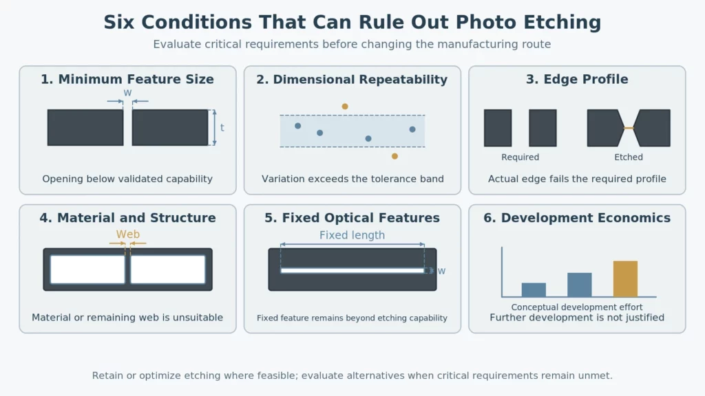
1. The Functional Opening Is Below the Validated Minimum Feature Size
Aperture dimensions must be evaluated at the boundary that controls the intended light path.
For an etched opening, the surface dimensions may differ from the actual unobstructed opening through the metal thickness. The relevant specification is therefore the functional opening defined by the customer.
If a required slit or pinhole cannot be formed at the specified thickness using the available etching process, the design falls outside the demonstrated manufacturing window.
Before abandoning etching, engineers can review whether an approved change in thickness, phototool compensation, or etching configuration would resolve the problem.
If the required opening remains unachievable, precision laser micromachining becomes a candidate for evaluation.
The decision should be based on the actual material and feature requirements rather than a universal numerical cutoff.
2. The Required Tolerance Cannot Be Maintained Reliably
A feature may be large enough to etch but still require a tolerance that exceeds demonstrated production capability.
Consider two hypothetical optical slits:
| Specification | Permitted width range |
|---|---|
| 0.100 ± 0.010 mm | 0.090–0.110 mm |
| 0.100 ± 0.002 mm | 0.098–0.102 mm |
Both designs have the same nominal width. However, the total permitted variation decreases from 20 μm to 4 μm in the second design.
The geometric feature has not changed, but the manufacturing and inspection challenge has.
This is why a statement such as “we can manufacture a 100 μm slit” is incomplete without the required tolerance and measurement definition.
For an etching route to remain suitable, the process must demonstrate acceptable dimensional variation against the approved specification.
The inspection system must also be capable of evaluating that variation. Measurement repeatability, reproducibility, calibration, and uncertainty are particularly relevant when acceptance limits are narrow.
If etching cannot achieve the required tolerance reliably, further process development or precision laser cutting should be evaluated.
3. The Etched Edge Profile Does Not Meet the Optical Requirement
An aperture can satisfy its nominal dimensions while failing a functional edge requirement.
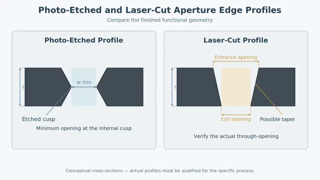
Photochemical etching removes material laterally as well as through the sheet thickness. Depending on the process configuration, the resulting edge may contain a tapered profile or an internal cusp.
Different etched cross-section configurations can be used to modify these profiles. The required outcome, however, must be confirmed for the actual component.
The first engineering question is whether the conventional etched profile is acceptable.
If it is not, the next step is to evaluate an alternative etching configuration or an approved design adjustment.
Only when these options cannot satisfy the required geometry should another machining process become the preferred candidate.
This is relevant when an optical design specifies a particular sidewall contour, limits internal edge projections, or requires a narrowly controlled light-transmitting boundary.
Precision laser cutting may provide a different edge profile, but its actual geometry must also be verified. It should not be assumed to produce perfectly vertical or defect-free sidewalls.
4. The Material or Remaining Metal Structure Is Unsuitable
Some aperture designs contain narrow metal webs between adjacent openings or long, unsupported sections of foil.
A design may appear feasible when the openings are evaluated individually, yet become difficult to manufacture when the remaining metal structure is considered.
The manufacturing review should include:
- Compatibility of the specified metal grade and condition with the etching process.
- Minimum remaining web width.
- Unsupported lengths and handling requirements.
- Part retention and separation from the processing sheet.
Established photo etching design rules link minimum land dimensions and component retention methods to the material thickness and geometry.
If a structural problem can be addressed through approved changes to the design or manufacturing support strategy, etching may remain appropriate.
However, if the specified material or required geometry is incompatible with the demonstrated etching process, an alternative manufacturing route should be considered.
Importantly, switching to laser cutting does not automatically resolve a weak component design.
A thin metal bridge that cannot tolerate normal handling may remain vulnerable regardless of how the surrounding openings are manufactured.
The cause of the problem must be identified before changing the process.
5. Critical Optical Features Cannot Be Modified
Design-for-manufacturing adjustments are useful only when they preserve the intended component function.
An engineer might improve etching feasibility by increasing a slit width or reducing the material thickness. For an optical instrument, however, those changes may affect the original design requirements.
For example, the entrance slit of a spectrometer participates in the trade-off between spectral resolution and light throughput. Different slit widths can therefore produce different instrument performance, as illustrated by the specifications of compact optical spectrometers.
A critical optical dimension should not be changed merely to accommodate a preferred manufacturing process.
If the approved slit width cannot be modified and etching cannot reproduce it, the correct engineering response is to investigate another qualified process.
This is one of the most important reasons to maintain access to precision laser cutting.
Manufacturing should adapt to the optical requirement whenever a suitable alternative is available—not require the optical design to adapt to the manufacturer’s preferred technology.
6. Further Etching Development Is Not Economically Justified
A component may be technically possible to etch but require extensive process development.
Multiple phototool revisions, additional trials, specialized inspection, and low initial yield can change the overall manufacturing decision.
The relevant comparison is the expected cost of delivering conforming components.
A simplified project-cost model is:
Total project cost = Setup + Processing + Development + Inspection + Post-processing
For an actual quotation, the evaluation should also account for scrap, rework, required quantity, and delivery schedule without double-counting costs already included in the manufacturing estimate.
The purpose of this model is not to establish a universal cost advantage for either technology. It is to compare the complete qualified manufacturing routes.
For a small development batch containing an unusually narrow slit, an already validated laser process may be more practical than extensive new etching development.
Conversely, a qualified etched design with numerous repeated openings may retain the economic advantages of sheet-based production.
An alternative process becomes attractive when the additional development required by etching is disproportionate to the project requirements.
Photo Etching Exit Criteria at a Glance
| Manufacturing condition | Retain or optimize photo etching | Evaluate an alternative route |
|---|---|---|
| Minimum opening | Within the validated feature range | Required opening cannot be formed reliably |
| Critical tolerance | Demonstrated dimensional control | Required variation cannot be maintained |
| Edge profile | Etched profile meets functional requirements | Critical edge geometry remains unacceptable |
| Material and structure | Compatible material and stable remaining features | Material or geometry is incompatible with the process |
| Design flexibility | Approved DFM adjustments can resolve the issue | Non-negotiable optical features remain unachievable |
| Development economics | Etching remains practical for the project | Further development introduces excessive cost or risk |
These conditions are decision points, not automatic instructions to switch to laser cutting.
The alternative process must still demonstrate that it can satisfy the same functional specification.
When Precision Laser Cutting Becomes the Better Alternative
Precision laser cutting becomes relevant when an optical aperture cannot be manufactured within the validated etching process window.
The objective is not simply to obtain a smaller hole. It is to reproduce the critical opening and edge geometry without compromising the rest of the component.
Precision Laser Micromachining for Narrow Optical Slits
Commercial optical instruments provide clear examples of laser-based aperture manufacturing.
The precision laser-cut slit and aperture assemblies used in Ocean Optics spectrometers are available in nominal slit widths ranging from 5 μm to 200 μm.
This demonstrates that precision laser cutting is an established manufacturing route for professional optical slits.
Specialized laser micromachining services also demonstrate the technical potential of laser processing for exceptionally narrow apertures.
However, the performance of specialized microfabrication systems should not be generalized to every laser cutting machine.
Conventional sheet-metal laser cutting and precision laser micromachining can involve substantially different optical configurations, focusing conditions, pulse characteristics, and material-removal mechanisms.
For example, femtosecond laser processing of metals uses extremely short pulses and can support localized microfabrication applications.
The appropriate laser route must therefore be selected according to the required feature and the available equipment.
What Must Be Verified After Switching to Laser Cutting?
Changing the manufacturing process does not change the aperture’s original functional requirements.
It changes the mechanisms used to achieve them.
Laser processing introduces its own dimensional and edge-quality considerations. The relevant laser cutting quality parameters include kerf width, kerf taper, thermal effects, surface finish, and residual material at the cut boundary.
| Laser processing characteristic | Why it matters for an optical aperture |
|---|---|
| Kerf width | Determines the width of material removed along a cut and influences achievable feature geometry |
| Kerf taper | Can produce different opening dimensions at the two surfaces |
| Heat-affected zone | May change the material condition near the cut edge |
| Recast or redeposited material | Can alter the intended opening boundary in processes where these effects occur |
| Edge condition | Influences the actual geometric boundary, cleanliness, and potential assembly requirements |
| Dimensional repeatability | Determines whether the critical opening can remain within specification across production |
The importance of each characteristic depends on the material, laser technology, processing parameters, and application.
For an optical slit, the final inspection must address the actual width over its specified effective length, rather than relying only on the programmed laser path.
A laser-cut feature should be accepted because it meets the drawing—not because it was produced by a technology generally associated with high precision.
What If Neither Etching Nor Laser Cutting Meets the Requirement?
Some optical apertures require geometries or tolerances that may be difficult to achieve through either available process.
In such cases, electroforming or specialized microfabrication methods may deserve consideration.
For example, research on ultra-narrow electroformed slit structures has demonstrated 5 μm-scale openings under specific experimental conditions.
Such results establish the feasibility of alternative microfabrication approaches, not a general production guarantee.
The manufacturing decision should remain open until a suitable process has been demonstrated.
Should the Entire Aperture Be Laser Cut, or Only the Critical Feature?
An optical component does not always need to be assigned to one manufacturing process based on its most difficult feature.
Consider a thin metal aperture plate containing several ordinary optical windows, two locating holes, and one exceptionally narrow slit.
Most of the geometry may be suitable for photochemical etching. Only the critical slit may require another process.
This creates three manufacturing options.
| Manufacturing route | When it is worth evaluating |
|---|---|
| Complete photochemical etching | All features fall within the validated etching process window |
| Complete precision laser cutting | Laser processing can meet the requirements of the complete component |
| Combined etching and laser processing | Most features suit etching, while a specific critical feature requires another operation |
Complete etching remains the preferred option to evaluate when it can satisfy all functional requirements.
If laser cutting is necessary for the critical opening, manufacturing the entire part by laser may simplify the production sequence by avoiding an additional process transfer.
A combined route may also be worth investigating. For example, the main component geometry could be etched, followed by laser processing of the critical opening.
However, this approach introduces additional engineering requirements.
The position of the laser-cut feature must be controlled relative to the etched mounting references. The thin component must be supported during the second operation, and previously manufactured features must be protected.
The drawing’s geometric dimensioning and tolerancing requirements provide the basis for maintaining consistent feature locations and functional relationships across operations.
The manufacturing sequence also needs to account for subsequent cleaning, surface treatment, and final dimensional inspection.
A combined process is therefore a candidate engineering solution that requires its own qualification. It should not be assumed to be more accurate or economical simply because it uses two technologies.
The right route is the simplest qualified process—or combination of processes—that can deliver the complete component.
Manufacturing Examples: Retaining Etching or Switching to Laser Cutting
The distinction between a suitable etched aperture and an aperture requiring an alternative process becomes clearer through two manufacturing scenarios.
TMNetch Case Example: Photo-Etched Copper Optical Apertures
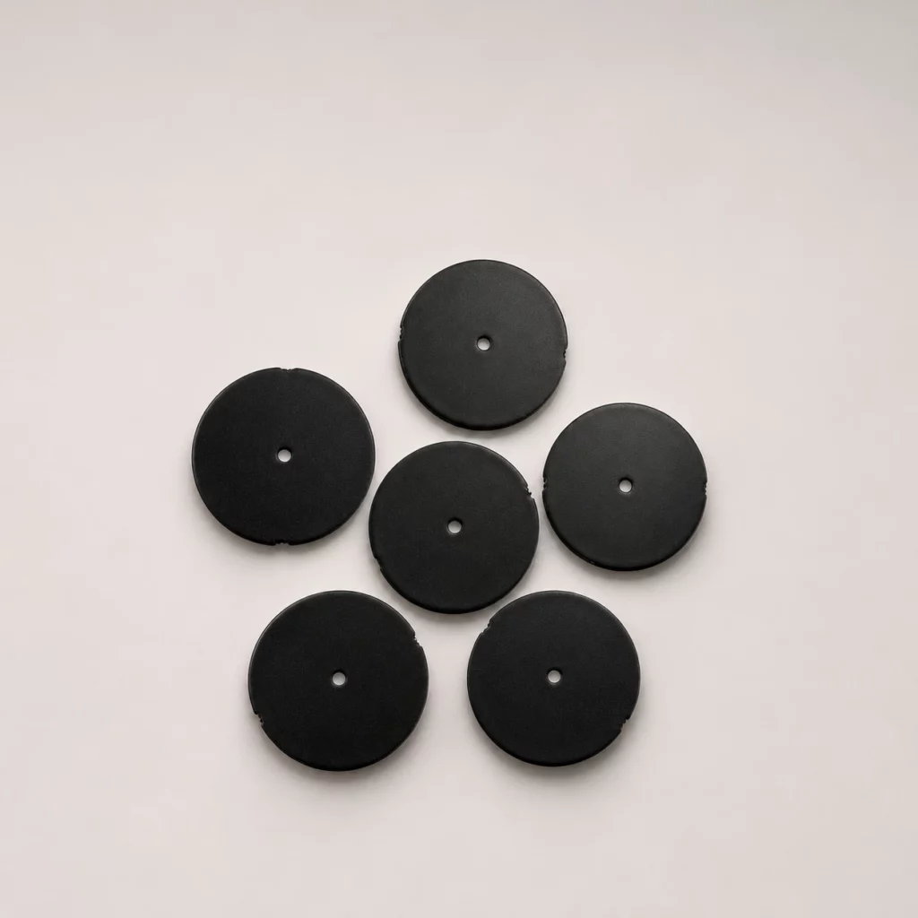
TMNetch has previously manufactured custom copper optical apertures with a matte black finish.
The components feature thin circular metal profiles and small central through-openings.
To protect customer-specific design information, the relevant manufacturing characteristics are summarized below:
- Material: Copper.
- Material thickness: Approximately the 0.1 mm range.
- Functional feature: Sub-millimeter central through-aperture.
- Component geometry: Circular thin-metal profile.
- Final surface condition: Matte black.
This application illustrates an important manufacturing principle: a professional optical component does not necessarily require laser micromachining.
For this type of copper aperture, photochemical etching provides a route for creating the internal opening and external profile within the same thin-metal component.
The manufactured parts demonstrate TMNetch’s experience with small optical openings, thin copper materials, and application-specific finished components.
The example also highlights why process selection should follow the geometry rather than the industry name. A component used in a precision optical assembly can still be a suitable candidate for etching.
The disclosed information is intentionally limited to the manufacturing characteristics of the project. Specific customer tolerances, optical performance, and inspection results are not presented.
Illustrative Engineering Example: A Narrow Spectrometer Slit
Now consider a different optical component.
Assume an engineer specifies a stainless steel foil aperture with the following requirements:
| Design parameter | Illustrative requirement |
|---|---|
| Material | Stainless steel foil |
| Thickness | 0.050 mm |
| Functional slit width | 0.010 mm |
| Slit length | 1.000 mm |
| Slit width tolerance | ±0.001 mm |
| Mounting features | Two locating or mounting holes |
| Design restriction | Critical slit width cannot be changed |
The opening-to-thickness ratio is:
w / t = 0.010 / 0.050 = 0.2
The required slit is also subject to a total width tolerance of only 2 μm.
These two conditions make the design a candidate for specialized manufacturing evaluation.
The first step is to determine whether the specified material, thickness, and functional slit width fall within an available, demonstrated etching process window.
If they do not, and the critical optical geometry cannot be adjusted, the next step is to evaluate precision laser micromachining.
The laser-produced sample must then be inspected for:
- Actual through-opening width.
- Width consistency along the specified slit length.
- Edge geometry and any relevant machining residues.
- Slit position relative to the mounting features.
This is an illustrative engineering example, not a TMNetch production case or a stated company capability.
Its purpose is to demonstrate the decision process when an optical aperture exceeds an available etching route.
What the Two Examples Demonstrate
The copper aperture illustrates a practical application of photochemical etching for a professional optical component.
The narrow slit example illustrates why an alternative manufacturing process may become necessary when a critical requirement exceeds validated capabilities.
The difference between the projects is not that one is an optical component and the other is more advanced.
It is that their required manufacturing windows are different.
One Manufacturing Partner, Multiple Process Options
A custom optical component should not be forced into a manufacturing process simply because that process is the supplier’s primary technology.
At TMNetch, photochemical etching remains our core manufacturing capability.
Our custom photo etching services support the production of precision metal components with custom opening patterns, external profiles, and integrated mechanical features.
For optical apertures and light shields, this provides the starting point for assessing material compatibility, feature geometry, and dimensional requirements.
However, when the required opening, edge profile, or tolerance cannot be achieved reliably through etching, we evaluate precision laser cutting as an alternative.
Where the available laser process can satisfy the approved drawing and inspection requirements, we can adopt that route instead of continuing to force an unsuitable etching solution.
TMNetch also provides in-house secondary manufacturing capabilities, including laser cutting services, metal bending, polishing, and surface finishing options.
This multi-process approach supports a manufacturing review based on the component’s requirements rather than the limitations of a single technology.
For an individual optical project, the choice may be complete etching, complete laser cutting, or another qualified manufacturing sequence.
The objective is to retain the advantages of photochemical etching wherever possible and introduce an alternative process only when it provides a better-supported route to the required component.
What to Include in an Optical Aperture Manufacturing Review
A manufacturing feasibility review is most effective when the supplier understands both the drawing requirements and the features that cannot be changed.
The following information helps determine whether photochemical etching remains the appropriate route or whether precision laser cutting should be evaluated.
| Required information | Purpose of the manufacturing review |
|---|---|
| Material grade and condition | Establish process compatibility |
| Metal thickness | Evaluate opening geometry and material-removal requirements |
| Smallest functional opening | Identify the most demanding aperture feature |
| Critical dimensional tolerances | Assess manufacturing and measurement capability |
| Required edge profile | Determine whether the resulting cross-section is acceptable |
| Non-negotiable optical features | Establish limits for design-for-manufacturing adjustments |
| Mounting and locating features | Maintain the required assembly relationships |
| Final surface condition | Define the state in which the component must be accepted |
| Sample and production quantity | Compare development requirements and production economics |
Before production, the supplier and customer should agree on how the critical opening will be measured.
An appropriate optical measurement system can be used to determine the boundary of a precision aperture. For applications requiring accurately known geometric areas, calibrated optical aperture measurement can provide a defined metrological basis.
Where the measurement result approaches a specification limit, the acceptance decision should follow the agreed rule for dimensional conformity and measurement uncertainty.
By establishing these requirements before selecting the process, engineers can evaluate alternative manufacturing routes without changing the original functional specification.
Our photo-etched optical components manufacturing services provide a starting point for this review, with precision laser cutting available for evaluation when critical features require an alternative approach.
Frequently Asked Questions
Is photo etching or laser cutting better for optical apertures?
Photochemical etching is particularly worth evaluating for thin-metal optical apertures with multiple openings, complex profiles, and integrated mounting features. Precision laser cutting becomes a candidate when a critical aperture dimension, tolerance, or edge profile falls outside the demonstrated etching capabilities. The appropriate process is the one that meets the complete functional specification.
When should an optical aperture be manufactured by precision laser cutting instead of etching?
Precision laser cutting should be evaluated when the required opening cannot be formed reliably by etching, when the critical tolerance cannot be maintained, or when the required edge profile cannot be achieved through an approved etching configuration. The laser process must then demonstrate compliance with the same drawing requirements.
Does precision laser cutting always produce smaller openings than photo etching?
No. Minimum feature size depends on the specific material, thickness, equipment, and process configuration. Specialized laser micromachining can produce exceptionally narrow optical slits, but conventional laser cutting equipment may not offer the same capability.
Can photo etching and laser cutting be used on the same optical component?
A combined manufacturing route can be evaluated when most features are suitable for etching but a particular critical opening requires laser processing. Such a route must be qualified for process sequencing, feature registration, part handling, and final inspection. It should only be selected when it offers a demonstrated manufacturing benefit.
Does TMNetch provide laser cutting when photo etching is unsuitable?
Yes. Photochemical etching is TMNetch’s primary manufacturing technology, and laser cutting is available as a complementary manufacturing capability. When etching cannot meet a project’s critical requirements, we evaluate precision laser cutting and use the alternative route when its feasibility has been established.
Conclusion
Selecting a manufacturing process for an optical aperture begins with the functional requirements of the component.
Photochemical etching is a valuable manufacturing route for complex thin-metal apertures, slit patterns, and light shields. Its ability to define multiple openings and mechanical features within a common patterned component makes it particularly worth evaluating for suitable optical designs.
However, the process must be assessed against the required opening size, material thickness, tolerances, edge profile, and production requirements.
When those requirements exceed the validated etching process window, precision laser cutting can provide an alternative manufacturing route.
At TMNetch, our approach is to retain the manufacturing advantages of photochemical etching wherever possible and evaluate alternative processes when necessary.
Have a custom optical aperture or precision slit design?
Submit your drawing to TMNetch for a manufacturing feasibility review and an evaluation of the appropriate photo etching or precision laser cutting route.