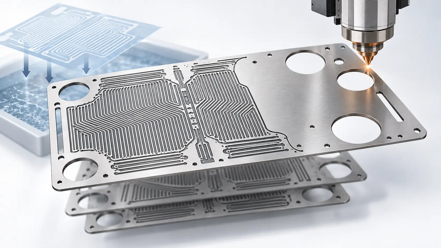

Custom lead frames are used when an electronic or semiconductor package needs a specific electrical path, thermal path, lead layout, material, plating, or package geometry. They are common in semiconductor and IC packaging projects, but they are also used in sensors, connectors, power devices, LEDs, medical electronics, automotive electronics, and industrial modules.
Standard lead frames may work for common package formats with low customization. A custom lead frame is usually needed when the project has special layout, reliability, thermal, electrical, or assembly requirements.
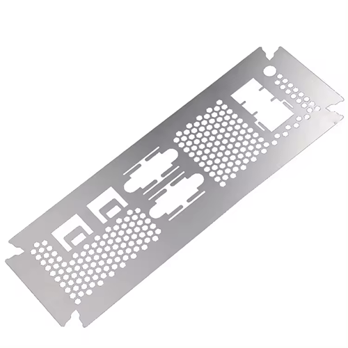
What Is a Custom Lead Frame Used For?
A lead frame is the metal frame in a package that provides external terminals and mechanical support. JEDEC defines a lead frame as a metal frame that provides external terminals and mechanical support in a package.
A custom lead frame is used when a standard frame cannot match the package design. It may include custom pin layout, lead pitch, lead width, die pad shape, bonding area, soldering area, plating area, or package outline.
Custom lead frames can support several functions:
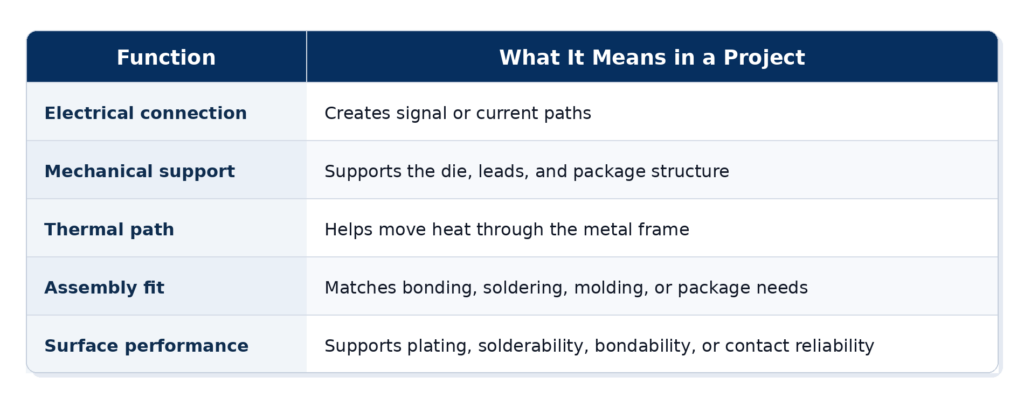
The final design depends on the device function. A power device lead frame may focus on current and heat. A sensor lead frame may focus on compact geometry and signal stability. A connector lead frame may focus on contact performance and plating.
Why Custom Lead Frames Matter in Semiconductor and IC Packaging
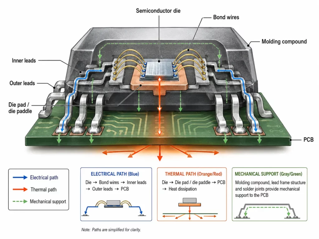
Semiconductor and IC packaging are core custom lead frame applications. In these projects, the lead frame is not just a piece of metal. It supports the die, creates the electrical path, helps manage heat, and provides the structure needed for package assembly.
A typical leadframe includes a die mounting paddle and lead fingers. The die paddle supports the die, while the lead fingers connect the die to circuitry outside the package.
Electrical connection from die to outside circuit
In a semiconductor package, the lead frame helps move signals or current from the die to the outside circuit. Wire bonds may connect the package leads with conductive pads on the die, so lead frame geometry and surface condition can affect assembly.
This is why an IC packaging lead frame may need custom lead width, pitch, bond pad area, die pad shape, or plating. If these details do not match the device structure, the package may face assembly or reliability problems.
Mechanical support during package assembly
A lead frame can also provide mechanical support during die attach, wire bonding, molding, trimming, forming, and final assembly. A custom lead frame design may be needed when the package has a special outline, compact footprint, or non-standard die pad.
Small geometry changes can affect how the part is handled in assembly. They can also affect lead alignment, molding stability, and package fit.
Thermal path for compact packages
Lead frames can also help move heat away from the die. This is especially important in power devices, LEDs, and compact IC packages.
Analog Devices notes that exposed die paddles in lead frame chip scale packages can help transfer heat from the component to the PCB and reduce thermal impedance.
For this reason, custom lead frames may be used when the die pad, thermal paddle, or metal path must support both electrical and thermal performance.
When Does a Semiconductor Project Need a Custom Lead Frame?
A semiconductor project may need a custom lead frame when the package has special electrical, thermal, mechanical, or assembly needs.
When a standard lead frame is not enough
A standard lead frame may not work if the package needs a non-standard pin layout, special lead pitch, custom die pad, special bonding area, or compact footprint.
It may also fall short when the device needs a specific current path, signal path, thermal path, or plating area. In these cases, custom lead frame applications are driven by package function rather than industry name alone.
In our production experience, buyers usually consider a custom lead frame when a standard frame cannot match the package layout, lead pitch, current path, thermal path, bonding area, soldering area, or material requirement. The decision should start from the device function, not from the manufacturing process alone.
When a standard or stamped lead frame may be enough
Not every project needs a custom lead frame. Standard lead frames may be enough for common package formats, standard materials, standard plating, and low customization.
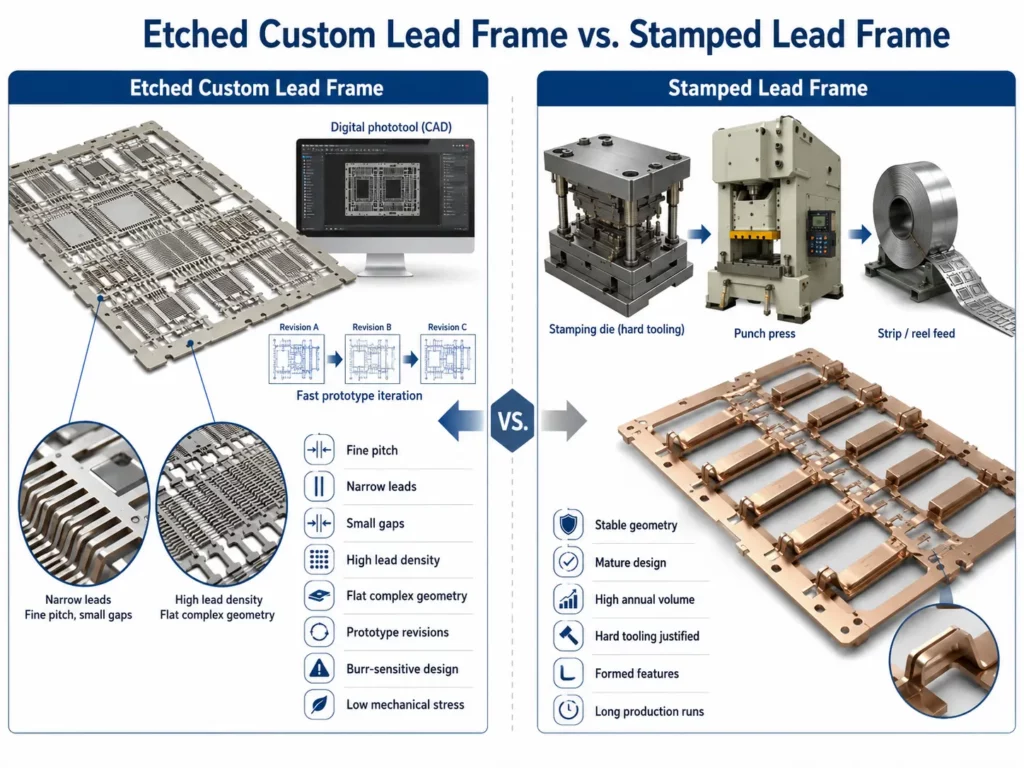
Stamped lead frames may also be suitable when the design is mature, the geometry is stable, annual volume is high, and hard tooling cost is justified. Stamping remains a practical process for many stable sheet metal parts, especially when die tooling and production scale support the part economics.
When custom design reduces downstream risk
Custom design can reduce risk when the package has fine pitch, special bonding areas, heat dissipation needs, or tight assembly limits. It can also help when the project needs specific inspection records, material certificates, or controlled surface finish.
For semiconductor lead frames, the key question is not only “Can this part be made?” It is also “Can this part support package assembly and long-term reliability?”
Main Industries That Use Custom Lead Frames
Custom lead frames are used across many electronics-related industries. Semiconductor and IC packaging remain the core application, but similar needs appear in sensors, connectors, power devices, LEDs, medical electronics, automotive electronics, and industrial modules.
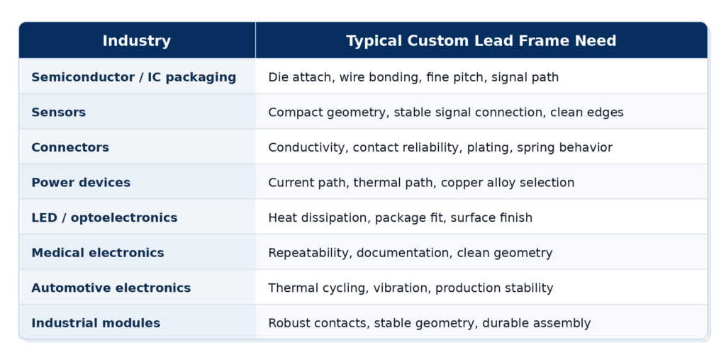
Semiconductor and IC packaging
Semiconductor lead frames support die attach, wire bonding, signal transfer, package structure, and thermal path. These projects may require fine pitch, stable lead geometry, clean edges, and controlled plating.
An IC packaging lead frame may also need a specific die pad size or shape. This is important when the package must support a special die size, exposed thermal pad, or compact footprint.
Sensors and MEMS-related packages
Sensor lead frame applications often need compact geometry and stable signal connection. Sensors may also need clean edges, controlled flatness, and repeatable dimensions.
For MEMS-related or precision sensor packages, the lead frame may need to support alignment and stable contact. Material stability can be important when the package is exposed to heat, vibration, or repeated use.
Connectors and electrical contacts
A connector lead frame or contact insert must support current flow, mechanical fit, and contact reliability. These parts may need copper alloys, phosphor bronze, beryllium copper, or plated surfaces.
The design may also need spring behavior, contact pressure, and stable mating performance. In these cases, custom lead frame design is closely linked to material choice and plating.
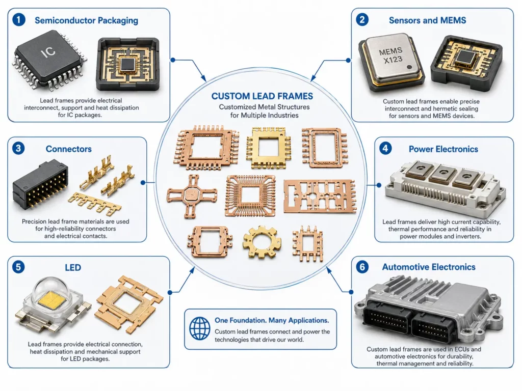
Power devices and energy electronics
A power device lead frame often needs a stable current path and thermal path. Copper-based materials are commonly reviewed because they can support conductivity and heat transfer.
Power modules, battery management systems, inverters, and control electronics may need thicker material, wider current paths, or larger die pad areas. Final design depends on current, heat, package size, and assembly method.
LED and optoelectronics
An LED lead frame can support the light source, provide electrical connection, and help move heat away from the package. Surface finish may also matter if the design has optical, soldering, or reflective requirements.
LED and optoelectronic packages often need compact layouts. Custom geometry may help when the package must fit into a small space.
Medical, automotive, and industrial electronics
Medical electronics may require repeatability, documentation, clean geometry, and stable signal connection. Automotive electronics may require production stability, vibration resistance, and thermal cycling performance.
Industrial electronic modules may need robust electrical contacts, stable geometry, and durable assembly. In all three areas, the application environment can be as important as the drawing.
Custom Lead Frame Applications by Project Type
Industry categories are useful, but project type gives a clearer engineering view. A custom lead frame may be needed for several different part functions.
IC packages and semiconductor devices
In IC packages, custom lead frames can support die pad geometry, leads, bond pads, wire bonding, molding, and package assembly. They help connect the internal die to the external circuit.
The design may change based on die size, number of leads, pitch, current path, and thermal path.
Sensor packages
Sensor packages may need a small footprint, stable signal path, clean edges, and low distortion. A custom lead frame can help when standard frames do not match the sensor layout.
The design may also need specific plating or surface condition for soldering, bonding, or contact reliability.
Electrical contacts and connector inserts
Electrical contacts and connector inserts need reliable conductive paths. Some designs also need spring response, plated contact areas, and repeatable mating surfaces.
For these projects, custom lead frames may look different from standard semiconductor frames. The key requirement may be contact performance rather than die attach.
Power device frames
Power device frames may need wider metal paths, thicker materials, or copper-based alloys. The design must support both electrical current and heat dissipation.
The die pad and lead geometry may need to match the current load and thermal path of the device.
LED lead frame structures
LED lead frame structures may support the light source, soldering surface, package body, and thermal path. The design may include a die pad, leads, plated surfaces, or reflective surface requirements.
Heat dissipation is often a key design factor. The lead frame must support both package fit and operating stability.
CTE-matched and hermetic package frames
Some high-reliability packages need controlled thermal expansion. For CTE-matched or hermetic package frames, buyers may consider controlled-expansion alloys such as Kovar or Alloy 42 when the metal must work with glass or ceramic sealing materials.
ScienceDirect describes Kovar as a nickel-cobalt ferrous alloy with a coefficient of thermal expansion similar to hard borosilicate glass, and also notes Alloy 42 in hermetic packaging contexts.
These materials are not selected mainly for high electrical conductivity. They are selected when expansion behavior, sealing compatibility, and package reliability are more important.
How Material, Plating, and Geometry Change by Application
Custom lead frame design depends on material, plating, and geometry. Buyers should not treat these as separate details. They work together.
Material selection
Lead frame materials should match the application. Copper alloys may be reviewed for conductivity and thermal performance. Phosphor bronze or beryllium copper may be reviewed for spring behavior. Nickel silver or stainless steel may be reviewed for corrosion resistance, strength, or stability.
For some CTE-matched packages, buyers may consider iron-nickel controlled-expansion alloys such as Alloy 42 or Kovar. The package design team should confirm final material choice.
Plating selection
Lead frame plating may affect solderability, bondability, contact reliability, and corrosion resistance. Common finishes can include tin, silver, gold, nickel, or other application-specific plating stacks.
The plating choice should match the assembly process. A wire bonding area, soldering area, or connector contact area may need different surface requirements.
Geometry and layout
Geometry includes lead pitch, lead width, gap, bridge width, die pad, tie bar, bonding area, soldering area, and package outline.
Small changes in geometry can affect assembly. Buyers should mark critical dimensions before RFQ so the manufacturer can review manufacturability.
When to Consider Etched Custom Lead Frames
This article is about applications, not only process selection. Still, etched custom lead frames can be useful in several project conditions.
Photo etched lead frames are produced through photochemical machining, a metal-etching process that uses photoresist to define where the metal will be etched.
Fine-pitch and high-density layouts
Etched lead frame designs may be useful when the package needs fine pitch, narrow leads, small gaps, or high lead density. These conditions often appear in compact semiconductor, sensor, and electronics packages.
Prototype and design iteration
Etched custom lead frames may also fit projects that are still changing. The buyer may need prototype samples, drawing revisions, or pilot validation before committing to a final production design.
In custom lead frame projects, etched designs are often reviewed when the part is thin, flat, complex, fine-pitch, or sensitive to burrs and mechanical stress.
Burr-sensitive and stress-sensitive assemblies
Some assemblies are sensitive to burrs, distortion, or mechanical stress. This can matter for wire bonding, soldering, flatness, and package alignment.
Etched custom lead frames may help when clean edges and low mechanical stress are important. The final choice still depends on material, thickness, geometry, tolerance, plating, and volume.
When stamping may still be suitable
Stamping may still be suitable when the design is mature, geometry is stable, annual volume is high, and hard tooling is justified. It may also be useful when the part needs formed features.
The best route should be selected after reviewing the drawing, material, quantity, package function, and assembly process.
Does Your Project Need a Custom Lead Frame?
Use this checklist before requesting custom lead frames.
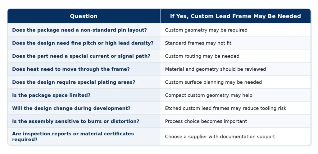
If several answers are “yes,” the project may need a custom lead frame. If the package uses a common layout, standard material, standard plating, and stable high-volume geometry, a standard or stamped frame may be enough.
Before RFQ, buyers should review how to choose a custom lead frame manufacturer and prepare the drawing, material grade, thickness, lead pitch, lead width, gap, die pad, plating requirement, tolerance, quantity, production stage, and application environment.
How TMNetch Supports Custom Lead Frame Projects
TMNetch supports chemical etched custom lead frames for semiconductor and electronics-related applications. Its Lead Frame page states that lead frames help establish electrical connections, provide mechanical stability, and optimize thermal performance in semiconductor manufacturing. The same page lists integrated circuits, LEDs, and semiconductor sensors as related application areas.
Custom lead frame manufacturing for semiconductor and electronics applications
For semiconductor and electronics projects, TMNetch can review the lead frame drawing, material, thickness, geometry, plating needs, tolerance, and production stage. This helps determine whether the design fits custom lead frame manufacturing.
The final route may depend on lead pitch, die pad design, bonding area, soldering area, flatness, quantity, and inspection needs.
Material and surface finishing support
TMNetch lists materials for chemical etched custom lead frames, including C17200 beryllium copper, CZ108 brass, C51000 phosphor bronze, 304/316 stainless steel, and C7521 nickel silver.
TMNetch also lists silver plating, gold plating, tin plating, and nickel plating for custom lead frames. These options may support solderability, bondability, corrosion resistance, or contact performance depending on the project.
Photo etching and chemical etching support
TMNetch’s Photo Etching page states that photo etching is stress-free and burr-free because no physical force touches the parts. It also lists tolerances as tight as ±0.025 mm.
TMNetch’s Lead Frame page lists precision down to ±0.025 mm, prototype lead frames within 6 hours, ISO 9001:2015 certified quality, dimensional reports, and material certifications.
Final suitability still depends on drawing, material grade, thickness, lead pitch, plating requirement, tolerance, quantity, and application environment.
Drawing review before production
For a practical review, contact TMNetch and send your drawing, material, thickness, lead pitch, plating requirement, tolerance, quantity, and application details.
A clear RFQ helps the engineering team review the package function, manufacturing route, inspection needs, and production stage.
FAQ About Custom Lead Frame Applications
What is a custom lead frame used for?
A custom lead frame is used for electrical connection, mechanical support, thermal path, and package-specific layout in electronic and semiconductor assemblies.
Which industries use custom lead frames?
Custom lead frames are used in semiconductor packaging, IC packaging, sensors, connectors, power devices, LEDs, medical electronics, automotive electronics, and industrial electronic modules.
Are custom lead frames used in semiconductor packaging?
Yes. Semiconductor lead frames support die attach, wire bonding, signal transfer, current paths, thermal paths, and package assembly.
When should buyers consider etched custom lead frames?
Buyers should consider etched custom lead frames for fine-pitch, high-density, thin, flat, burr-sensitive, or design-changing projects.
When is a standard or stamped lead frame enough?
A standard or stamped lead frame may be enough when the project uses a common package format, stable geometry, standard material, standard plating, and mature high-volume production.
Conclusion
A custom lead frame is useful when a semiconductor or electronics package needs a specific electrical path, thermal path, material, plating, lead pitch, pin layout, or package geometry.
Semiconductor and IC packaging are the core applications, but similar needs also appear in sensors, connectors, power devices, LEDs, medical electronics, automotive electronics, and industrial modules.
Standard or stamped lead frames may work for stable, common, high-volume designs. Custom or etched custom lead frames may fit compact, fine-pitch, high-density, burr-sensitive, or design-changing projects.
To review a project, send your drawing, material, thickness, plating requirement, tolerance, quantity, and application details to TMNetch.