
A lead frame is a key metal structure used in semiconductor packaging. It supports the silicon die, provides electrical pathways between the chip and external circuits, and helps transfer heat away from the device during operation.
For engineers and buyers, understanding how a lead frame works helps them make better decisions about design, materials, manufacturing, and sourcing. As semiconductor packages become smaller and more complex, lead frame design and fabrication quality become more important. They can directly affect electrical performance, thermal management, assembly reliability, and production cost.
This guide explains what a lead frame is and why it matters in semiconductor devices. It also compares key design factors, lead frame types, materials, package styles, manufacturing processes, and common applications.
What Is a Lead Frame?
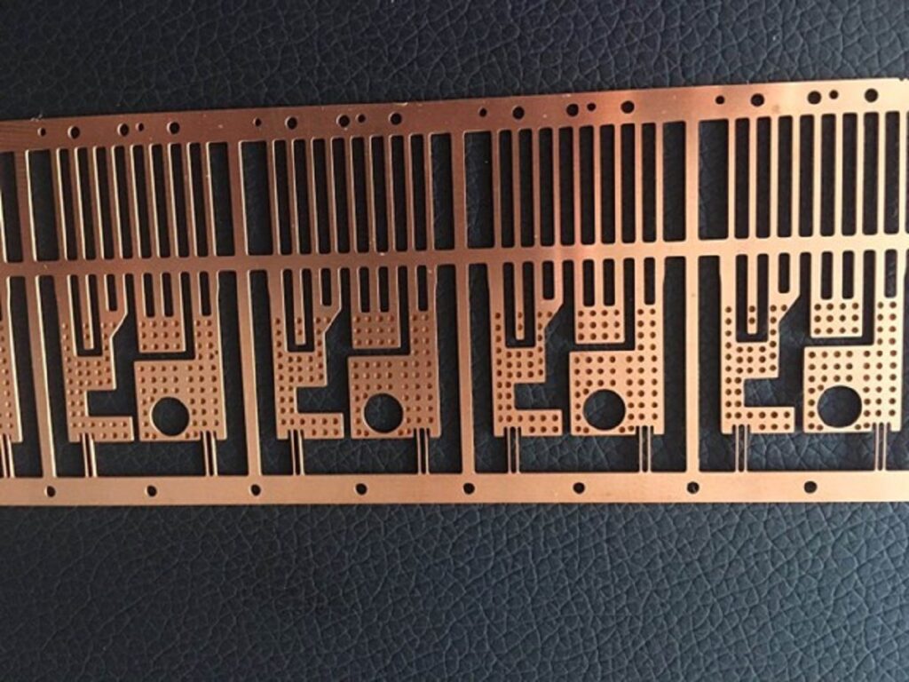
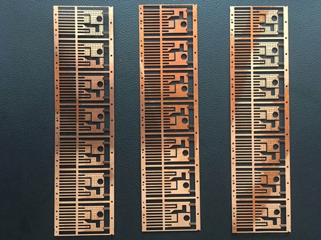
A lead frame is a precision metal structure used inside an electronic package. It holds the semiconductor chip and connects it to external circuits. It also supports the die and helps create stable electrical connections between the chip and the outside system. In most semiconductor packages, lead frame precision can directly affect signal performance and heat dissipation.
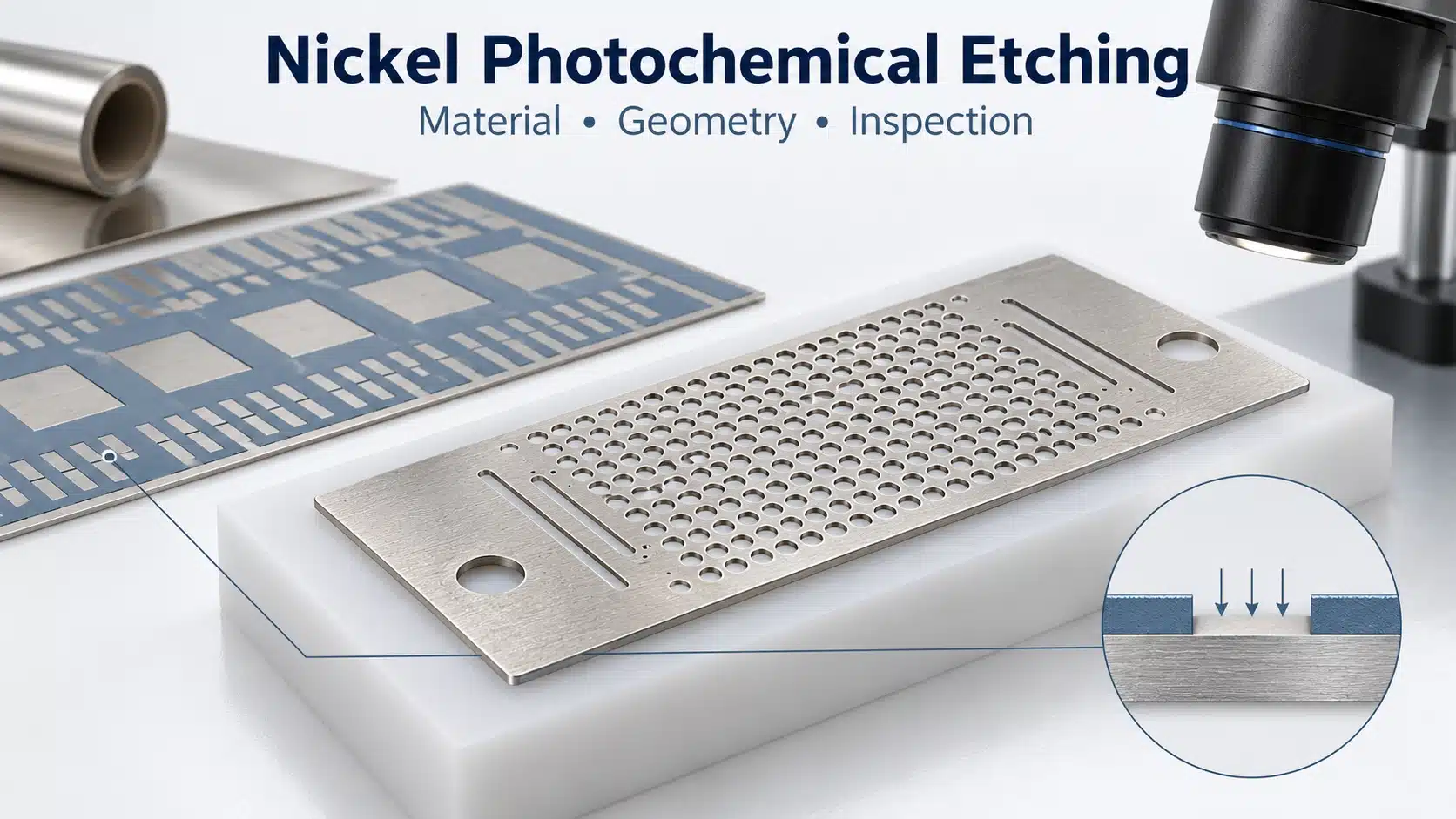
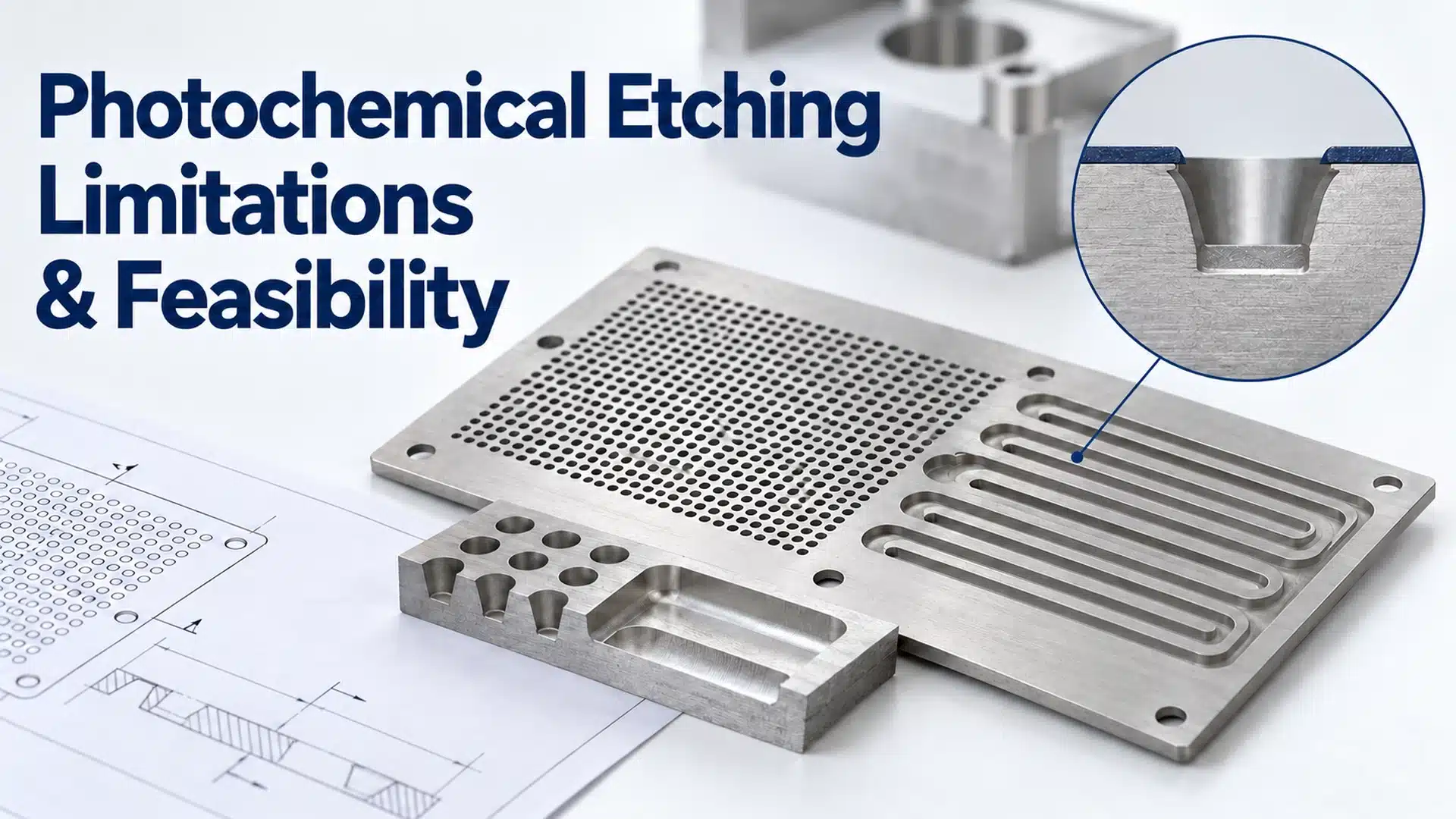
Modern semiconductor packages typically demand tighter dimensional control, which is one reason manufacturers use custom lead frame designs to meet mechanical, electrical, and thermal requirements. For fine-pitch and complex lead frame geometries, photo etching provides a tooling-free manufacturing option without introducing mechanical cutting stress.
A precision standard that photo etching is uniquely positioned to achieve.
The Role of Lead Frames in Semiconductor Devices
In semiconductor devices, the lead frame plays a central role in both structure and performance. It holds the silicon die in place, connects the chip to the external circuit, and helps manage heat during operation. Without a stable lead frame, the package may face problems such as poor electrical contact, weak mechanical support, or reduced thermal reliability.
The lead frame in semiconductor also helps protect the chip during assembly and use. During die attach, wire bonding, molding, and final packaging, it provides a stable metal base for the semiconductor die and its connection points. This stability is important because even small dimensional changes can affect bonding quality, package alignment, and long-term device performance.
For modern semiconductor packages, lead frames must support smaller sizes, higher pin counts, finer lead pitch, and better heat dissipation. This is why the design, material, thickness, surface finish, and manufacturing method of the lead frame all need to be carefully controlled. A well-designed lead frame can improve electrical performance, support reliable assembly, and help extend the service life of the final device.
Key Elements and Functions of a Lead Frame
A lead frame is more than a simple metal carrier. It combines mechanical support, electrical connection, heat transfer, and package compatibility in one precision metal component. In semiconductor packaging, each element of the lead frame must be carefully designed to support stable assembly and long-term device performance.
Mechanical Support for the Die
The die pad provides a stable base for the silicon die during die attach, wire bonding, molding, and final packaging. This support helps keep the die in the correct position and reduces the risk of movement during assembly. For small, high-density packages, stable die support is important. It helps ensure reliable bonding and accurate package alignment.
Electrical Pathway Formation
The lead fingers form conductive paths between the die and the external circuit. Inner leads connect to the chip through bonding wires, while outer leads connect the package to the PCB or other electronic systems. Good lead frame design helps maintain stable signal transmission and electrical performance.
Thermal Management Capability
A lead frame also helps transfer heat away from the semiconductor die. This is especially important in power devices, automotive electronics, LEDs, and other performance-critical applications. A copper alloy lead frame is often selected when the package needs better electrical and thermal conductivity.
Package Compatibility
Lead frames are used in many semiconductor package types, including QFP, QFN, SOP, and DIP packages. The lead pitch, lead count, frame thickness, and die pad layout must match the package design and assembly process. Good package compatibility helps improve production efficiency and supports automated assembly lines.
Precision Manufacturing Control
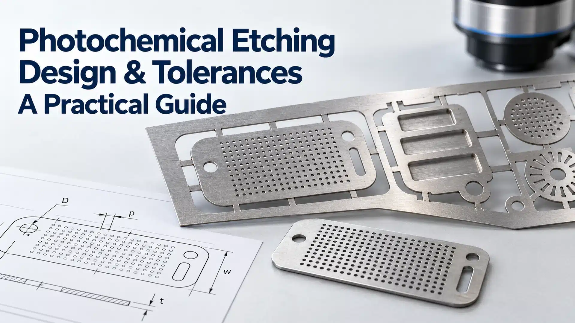
Dimensional accuracy is critical in precision lead frame manufacturing. Small changes in lead pitch, lead width, or frame thickness can affect wire bonding quality, package alignment, and final assembly yield. Engineers should therefore review photochemical etching tolerances and design limits against material thickness, lead geometry, feature density, and inspection requirements before releasing a lead frame drawing for production.
Design Customization
Custom lead frame fabrication allows engineers to adjust the die pad size, lead finger layout, lead count, frame thickness, and surface finish based on electrical, thermal, and mechanical requirements. This flexibility is useful for custom IC packages, sensors, power devices, and other semiconductor applications where standard lead frames may not fit the design.
Surface Performance and Plating
A plated lead frame can improve solderability, wire bonding performance, corrosion resistance, and electrical contact quality. Common surface finishes may include silver, nickel, tin, or gold, depending on the final application. Proper plating control is important for stable assembly and long-term package reliability.
Manufacturing Reliability
Lead frame fabrication must remain consistent from prototype to batch production. Stable manufacturing helps reduce burrs, dimensional variation, plating defects, and assembly problems. For fine features or complex patterns, an etched lead frame produced by precision metal etching can support clean edges, flexible design changes, and burr-free lead frame production.
Cost and Material Efficiency
A well-designed lead frame balances material use, package performance, and production cost. The goal is not only to reduce metal waste, but also to maintain strength, conductivity, thermal performance, and dimensional stability. This balance is important for both prototype development and high-volume semiconductor production.
Long-Term Performance Stability
A reliable lead frame must withstand heat, mechanical stress, bonding forces, and environmental changes during the product life cycle. When the material, design, plating, and manufacturing process are properly controlled, the lead frame can support stable electrical performance, better thermal reliability, and longer device service life.
Types of Lead Frames and Common Materials
The mold is formed by a metal frame with various designs and materials for different semiconductor package needs. The optimal design of structure and material is crucial for electrical performance, heat dissipation, and process ability. For such advanced designs, there are even controlled lead frame manufacturing processes and specific metal frame that serve special application purposes.
By Manufacturing Method
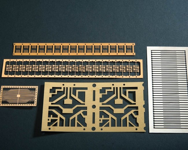
Most lead frames are made by stamping or chemical etching. Stamping uses hard tooling to cut and form metal strips. Chemical etching removes selected metal areas through a controlled chemical process.
- Stamped Lead Frames: These are produced through a stamped metal frame process, which is best for high volume.
- Etched Lead Frames: Fine patterns and close tolerances can be achieved using chemical etching. It is the choice for complicated layouts and high-density packages.
-Based on TMNetch process capability data, chemical etching can process metal sheets from 0.01 mm to 2.5 mm. Fine accuracy can reach ±0.025 mm under suitable design conditions. Final tolerance still depends on material, frame thickness, lead pitch, and pattern density.
In simple terms, stamping is often better suited to mature, stable designs produced at very high volumes. Chemical etching for custom lead frame fabrication can be more suitable for fine-pitch geometries, complex patterns, rapid design changes, and early-stage development.
By Package Type
Package type affects the die pad, lead fingers, lead count, and connection method. It also affects how the lead frame fits the PCB and assembly process. A reliable semiconductor lead frame supplier should confirm the package type before production.
QFP and QFN packages usually require tighter dimensional control because they use finer pitch and higher lead density. SOP and DIP packages are generally easier to assemble, but plating quality and lead consistency still matter.
Common Materials
- Copper Alloy Lead Frames: Copper-based alloys also have a high degree of electrical and thermal conductivity. They are extensively used in performance-oriented semiconductor systems— for precision Copper Etching solutions, TMNetch maintains tight tolerances across all alloy grades.
- Iron-Nickel Alloy Lead Frames: These materials also have a high degree of mechanical integrity and controllable expansion. They are used in applications where high accuracy is necessary, and benefit from precision Nickel Etching processes that preserve tight dimensional control.
- Custom Material Lead Frames: Special alloys or coatings may be combined using a custom lead frame. This is beneficial in that it allows the introduction of details for electrical, thermal, or environmental purposes.
Lead Frame Manufacturing Process: Step-by-Step Guide
The lead frame manufacturing process is a high-precision, repetitive process used to fabricate quality housing frames of metal for semiconductor packaging. Every phase is focused on precision, such as the material and quality of lead frame fabrication services in many cases, meeting society standards.
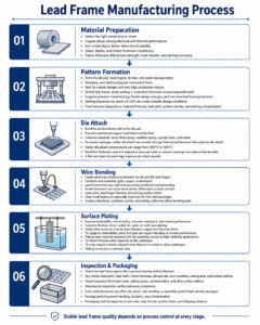
Material Selection and Preparation:
The process starts with selecting the right metal strip or sheet. Copper alloys are common when the package needs strong electrical and thermal performance. Iron-nickel alloys are used when dimensional stability is more important.
Before pattern formation, the material must be cleaned, flattened, and checked for thickness consistency. Frame thickness affects lead strength, heat transfer, and etching accuracy.
–TMNetch’s chemical etching can process metal sheets from 0.01 mm to 2.5 mm.Pattern Formation:
Pattern formation creates the die pad, lead fingers, tie bars, and outer lead geometry. Stamping uses hard tooling and mechanical force. It is efficient for mature designs with very high production volume.
For an etched lead frame, the pattern is transferred onto the metal with photo tooling. Then, controlled chemicals remove the exposed metal areas. This process supports precision metal etching, flexible design changes, and burr-free lead frame production.
–TMNetch’s etching tolerance can reach ±0.025 mm under suitable design conditions. For a tight tolerance lead frame, the final result still depends on material thickness, lead pitch, pattern density, and etching compensation.
Die Attach:
Die attach means bonding the semiconductor die to the die pad. This step provides mechanical support and helps transfer heat from the chip to the lead frame. Common die attach materials include silver-filled epoxy, modified epoxy, cyanate ester, and solder.
For power packages, solder die attach can provide stronger thermal performance than polymer die attach. Industry packaging data shows solder die attach temperatures can range from 260°C to 345°C. Bond line thickness control is also important because voids or uneven coverage can reduce heat transfer.
A flat and clean die pad helps improve die attach quality. If the lead frame has poor surface condition, weak plating adhesion, or dimensional variation, the die may not sit correctly. This can affect later wire bonding and molding reliability.
Wire Bonding:
Wire bonding creates electrical connections between the die and the lead fingers. Gold, copper, or aluminum wires are commonly used, depending on the package design and cost target. Each wire usually connects one bond pad on the die to one bonding area on the lead frame.
During bonding, the lead frame must stay rigid and accurately positioned. Small movement can cause weak bonds, lifted wires, or poor contact. This is why lead pitch, lead finger flatness, and plating quality matter in precision lead frame manufacturing.
For fine-pitch packages, clean lead fingers are especially important. A reliable semiconductor lead frame supplier should control surface cleanliness, oxidation, and plating uniformity before assembly. These details directly affect bonding yield.
Surface Plating Treatment:
Surface plating improves solderability, wire bonding, corrosion resistance, and contact performance. A plated lead frame may use silver, nickel, tin, gold, or multi-layer finishes. The right finish depends on bonding method, soldering process, storage condition, and final application.
Nickel often works as a barrier layer between copper and the outer finish. Tin supports solderability, while silver and gold can support bonding or contact performance. In high-reliability applications, the plating stack must be reviewed with the assembly process.
Industry guidance shows that tin finish thickness often depends on the underlayer. For example, tin may require a thicker deposit when there is no nickel or silver underlayer. This is why plating should not be treated as a simple cosmetic step.
For etched parts, the usual process route is etch first and plate after etching. This helps avoid uneven etching through pre-plated metal layers. For projects requiring silver, nickel, tin, gold, or other finishes, TMNetch’s metal plating services for precision etched parts can be incorporated into the post-etch manufacturing workflow.
Inspection & Packaging:
Inspection checks whether the lead frame meets the drawing before shipment. Important checkpoints include lead pitch, lead width, frame thickness, die pad size, burr condition, plating area, and surface defects. For custom lead frame fabrication, dimensional inspection should match the critical features on the customer drawing.
Visual inspection can find surface defects, bent leads, plating issues, and contamination. Dimensional inspection verifies whether the part meets tolerance requirements. For high-density packages, even small deviation can affect die attach, wire bonding, or final assembly yield.
After inspection, lead frames must be packed to prevent bending, oxidation, and contamination. Packaging method depends on part size, strip format, surface finish, and shipping distance. Good packaging helps the lead frame supplier protect precision parts until they reach the assembly line.
Etched Lead Frames: Precision Solutions by TMNetch
Etched lead frames create very fine dimensions in complex semiconductor designs that require tight tolerances and small geometries.
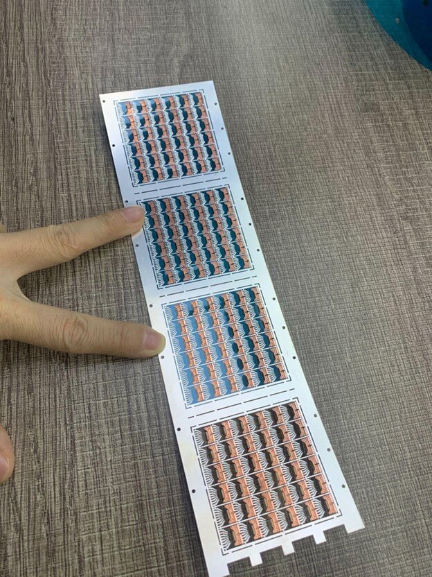
- High-Precision Patterning: Etching provides an ultra-fine pitch to enable fine-pitch packaging and stable electric properties.
- Optimized for Complex Designs: Custom lead frames are practical when an application calls for a specific the structure design, often because of performance or space constraints.
- Controlled Lead Frame Manufacturing Process: With tight process control, TMNetch can guarantee uniform thickness, a clean edge, and repeatable quality.
- Enhanced Reliability and Yield: Accuracy of etching minimizes mechanical stress and enhances the long-term reliability of a package in critical applications.
- Scalable Fabrication Support: “TMNetch’s lead frame fabrication services are well-suited for prototyping or high-volume production and do not sacrifice precision.
Applications of Lead Frames in Modern Electronic Devices
Lead frames are widely used alongside other precision etched electronic components in semiconductor and electronic assemblies. They provide structural support, electrical connectivity, and a thermal path from the integrated circuit die or chip to the surrounding package.
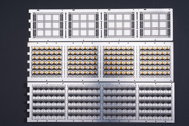
Consumer Electronics: Smartphones, laptops, and wearables rely on precision etched electronic components for compact mounting and reliable electrical connectivity.
- Automotive Electronics: Also in the automotive sector, control modules and sensors are driven by durable packaging, including, as a rule, customer-specific L/F solutions for most harsh environments.
- Power Management Devices: Provides high-end electrical performance that is reliable on the job.
- Industrial Equipment: Lead frames support industrial automation applications where stamped manufacturing delivers consistent throughput at high volume.
- Mass-Produced Electronic Components: PCB etched metal frames offer precision and intricate custom features in semiconductor devices with the smallest dimensions.
FAQs
1. What is a lead frame?
A lead frame is a precision metal structure used in semiconductor packaging. It supports the silicon die, provides electrical paths through the lead fingers, and helps transfer heat away from the chip. In most packages, the lead frame connects the internal semiconductor device to the external circuit.
2. What does a lead frame do in semiconductor devices?
A lead frame provides mechanical support, electrical connection, and thermal management. The die pad holds the silicon die in place, while the lead fingers connect the chip to the outside circuit. A stable lead frame helps improve bonding quality, package reliability, and long-term device performance.
3. When should manufacturers choose a custom lead frame?
A custom lead frame is the perfect solution when off-the-shelf options are unable to match the required electrical, thermal, or package needs. Performance may be further optimized for advanced or high-reliability semiconductor applications through customization of the metal frame process.
4. Why is stamped lead frame manufacturing widely used?
Stamped lead frame manufacturing is preferable, especially for high-speed, precision, and low-cost production. Choosing a reliable semiconductor frame for semiconductor manufacturer for the precise tooling, consistency of quality, and large production volume.
Conclusion
A lead frame is one of the most important components in semiconductor packaging that significantly determines electrical performance, thermal management, and mechanical stability throughout its lifetime. Choosing the correct lead frame manufacturing process means consistent quality in low to high-volume production. For more sophisticated applications, a custom lead frame provides flexibility and performance. Teaming with experienced suppliers of lead frame fabrication services, such as TMNetch, effectively reduces the burden on manufacturers for production risk by offering a proven yield. Choosing the best lead frame semiconductor supplier is critically important for achieving mature, high-performance devices in a commoditizing electronics marketplace.
Need a custom etched lead frame for your semiconductor package?
Send us your drawing, material type, frame thickness, lead pitch, lead count, plating requirement, and estimated quantity. TMNetch can help review whether precision metal etching is suitable for your lead frame design.