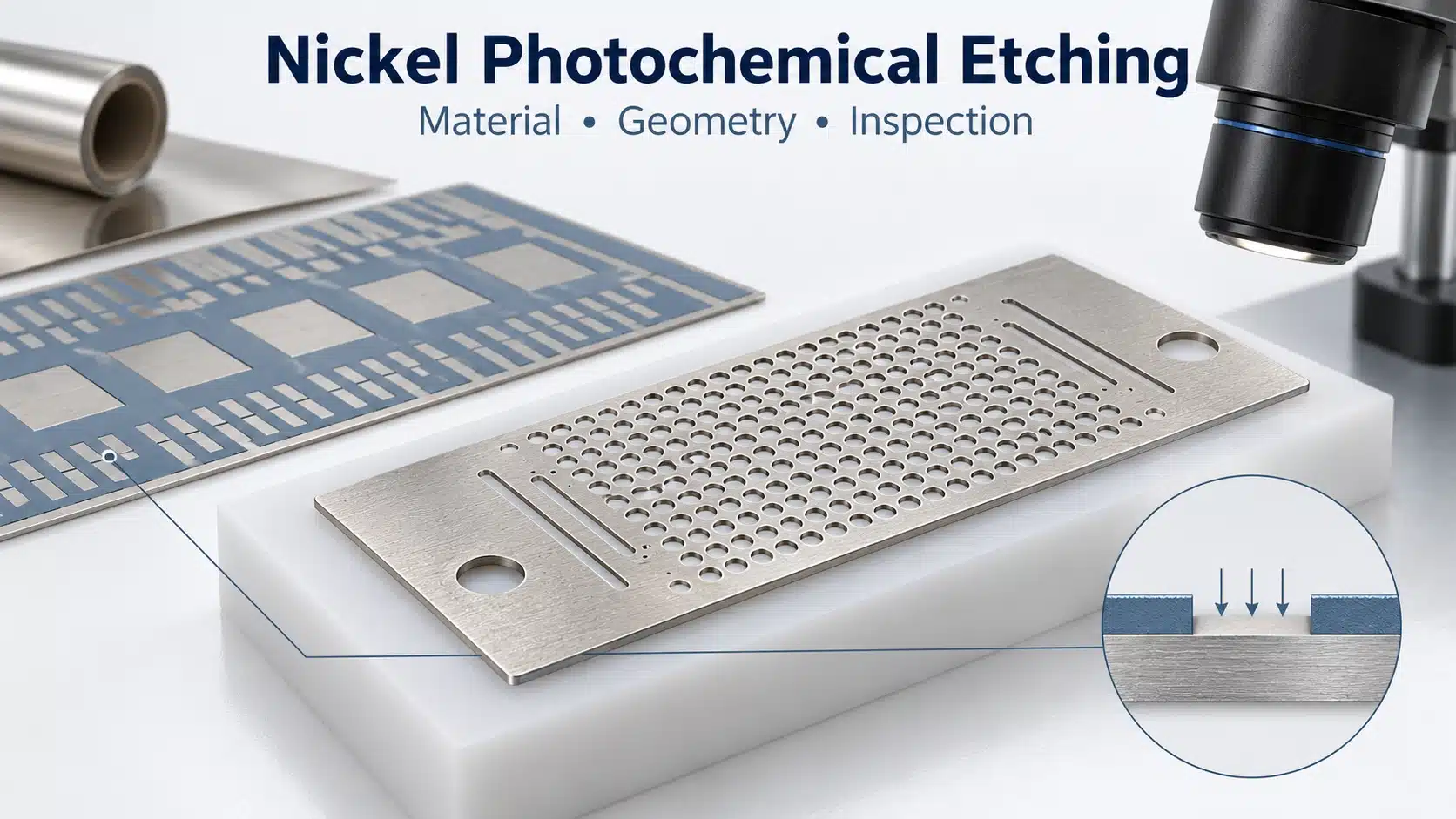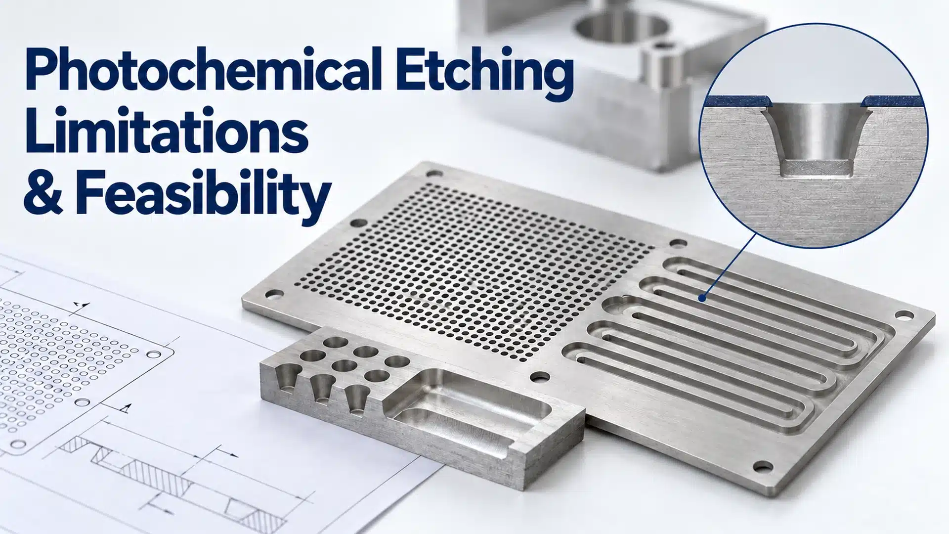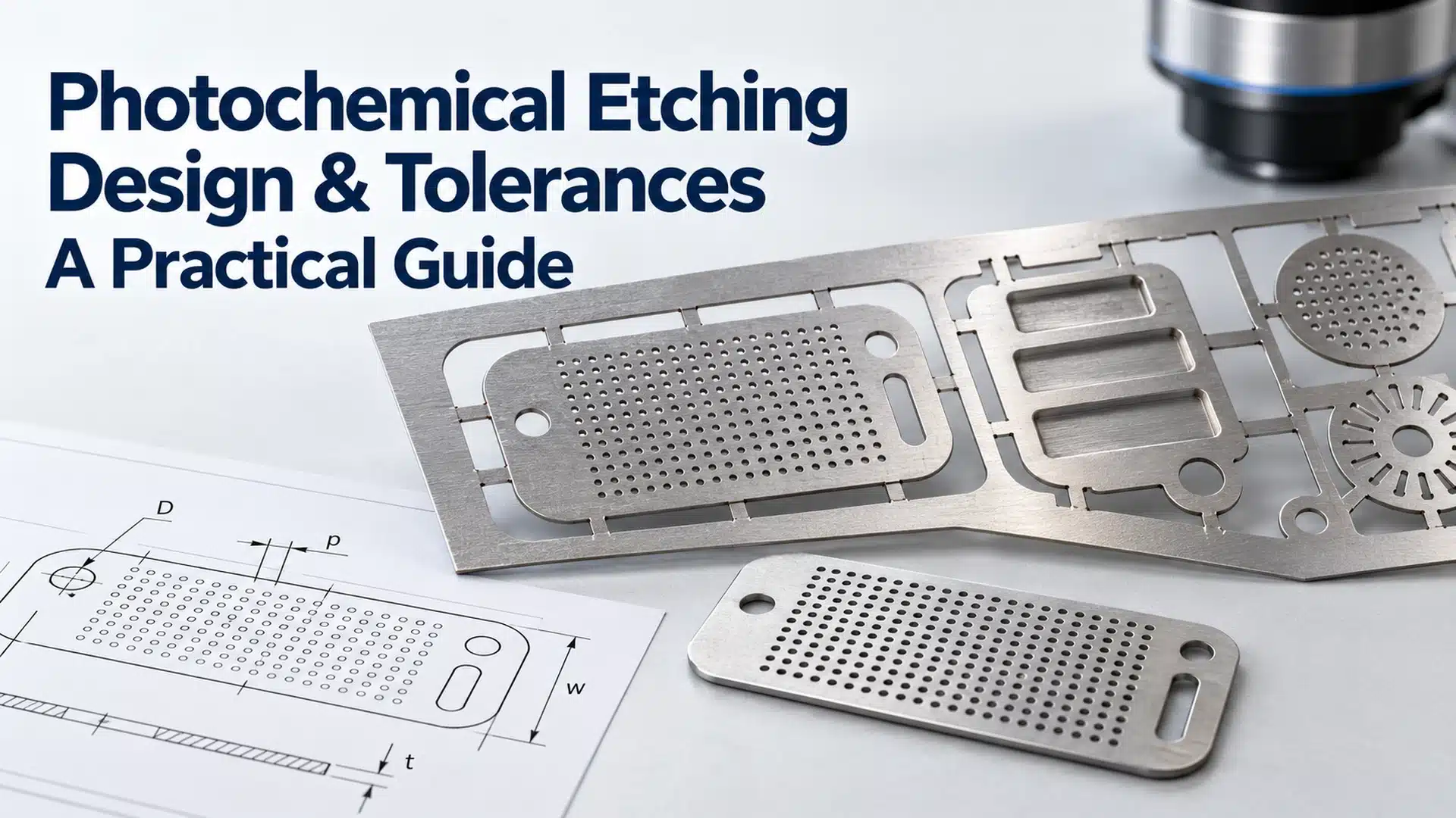

Industrial copper etching is used in many fields, from decorative copper plate etching to precision industrial manufacturing. For engineers and buyers, the key concern is not only how copper is etched, but whether the process can produce accurate, burr-free, and repeatable copper parts for real applications. Industrial copper chemical etching uses controlled photoresist, exposure, development, and etching steps to create fine copper features without mechanical stress or heat damage. This makes it suitable for electrical contacts, EMI shielding parts, lead frames, connectors, heat spreaders, copper mesh, and other custom copper etched components. In this guide, we explain the copper etching process, suitable copper materials, design factors, common applications, and how to choose a reliable copper etching supplier for prototype and volume production. For companies comparing copper etching services, the main value of precision copper etching is stable part quality across prototype and volume production.
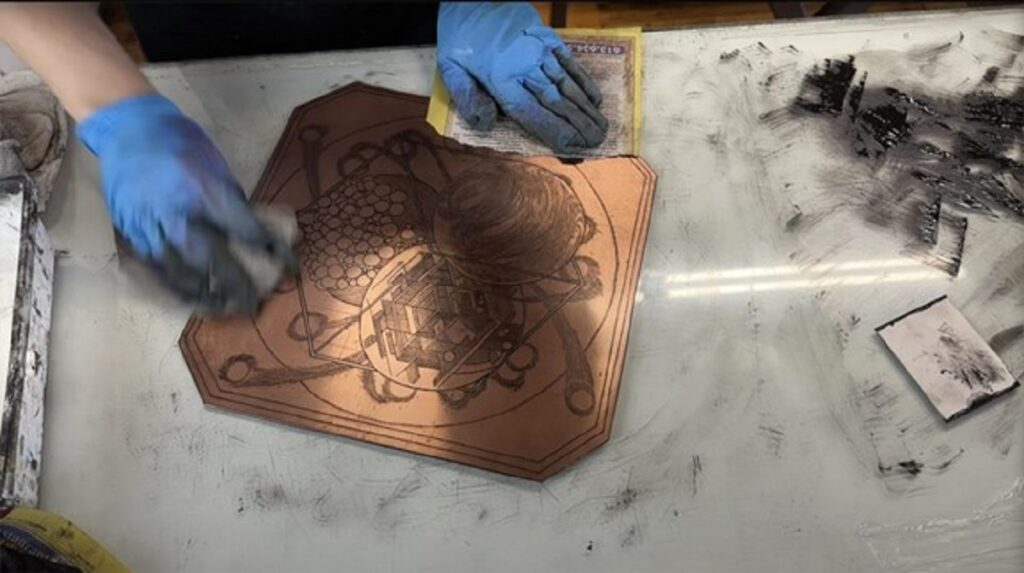
What is Copper Etching?
Copper Etching involves removing layers of copper in a controlled manner through a chemical etching process to create designs, patterns, or functional components. It has a history in printmaking, but today it remains just as important in electronics, jewelry, and industrial applications.
Key Features of Industrial Copper Etching
- Supports copper chemical etching for thin, flat, and detailed copper parts.
- Creates photo etched copper components with fine holes, slots, and complex outlines.
- Helps achieve burr-free copper etching without stamping force.
- Supports stress-free copper etching because the process does not use laser heat.
- Works well for custom etched copper components used in electronics and shielding.
Copper Etching Process
The copper etching process removes selected areas from a copper sheet through controlled chemical reaction. In industrial production, this method is also called copper chemical etching, copper photo etching, or photochemical etching copper.
Unlike stamping or laser cutting, chemical etching copper parts does not use mechanical force or heat. This helps produce burr-free copper etching results, stress-free copper etching edges, and stable dimensions for precision copper components.
For buyers, the key point is not only how copper is etched. The real question is whether the copper etching manufacturer can control material thickness, line width, etch depth, tolerance, surface finish, and inspection consistency. Engineers should also review photochemical etching tolerances and design limits before finalizing copper part designs.
Based on TMNetch’s production capability, copper etching can process copper foils and plates from 0.05 mm to 2.5 mm. The maximum part size can reach 1500 × 600 mm, and suitable designs can achieve tolerances as tight as ±0.03 mm.
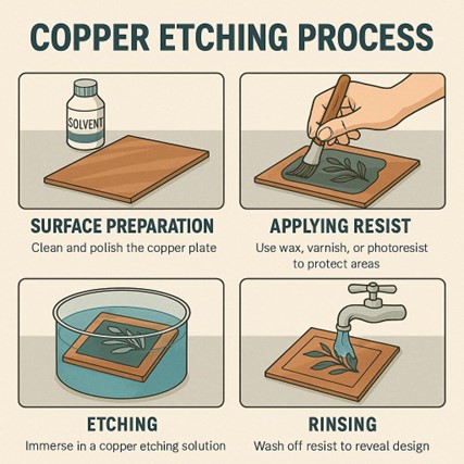
Step 1: Surface Preparation
Surface preparation decides whether the photoresist can bond evenly to the copper sheet. Photoresist is a light-sensitive protective layer that controls which areas stay and which areas are etched.
Before precision copper etching, the copper surface must be cleaned to remove oil, dust, oxide, and fingerprints. Poor cleaning can cause pinholes, uneven etching, weak adhesion, or local over-etching.
For copper electrical contacts, copper EMI shielding, copper connectors, and copper lead frame parts, this step is especially important. Small surface defects can affect conductivity, bonding quality, and final assembly performance.
Step 2: Apply and Design The Resist
Choose a resistance that aligns with your goals and level of expertise:
- Hard ground: Traditional asphaltum‑based layer for sharp lines with needles. Heat is applied; scratches reveal copper for etching. It is great for engraving with high levels of detail, like a copper plate etching.
- Soft ground: Tacky coat picks up textural (fabric, leaves) and makes tonal, sketch-style lines.
- Acrylic or enamel paint: Slightly more difficult to use: brush-on masks for large areas and stop-outs.
- Photoresist Film: A reflective film designed for optimal resolution halftones, PCBs, and detailed text. Expose with UV and develop using a sodium carbonate solution, perfect for accuracy in the copper etching process.
- Toner transfer: This method involves printing your artwork in reverse on a glossy medium and then heat-transferring it onto the plate; it is particularly suitable for rapid circuit creation.
Let the coatings cure fully. Any tackiness leads to undercutting later.
Step 3: Mask Edges, Back, and Mount
The non-etched areas must be protected before the sheet enters the etching line. This may include the back side, border area, tooling holes, or special contact points.
For single-sided etching, only one surface receives controlled material removal. For double-sided or multi-depth etching, both sides must align carefully to control opening size, depth, and edge profile.
This matters for etched copper components such as copper busbars, copper shielding components, copper heat spreaders, and fine copper mesh. Misalignment can affect current flow, shielding performance, or thermal contact area.
Step 4: Prepare and Condition the Etchant
The etchant is the chemical solution that dissolves exposed copper. In industrial copper alloy etching, the supplier must control concentration, temperature, spray pressure, and line speed.
Copper reacts differently from brass, phosphor bronze, beryllium copper, nickel silver, and oxygen-free copper. Each alloy needs suitable process settings to reduce undercut, staining, and dimensional variation.
This is why professional copper etching services do not rely on one fixed recipe. A reliable copper etching manufacturer adjusts the process based on material grade, thickness, pattern density, and drawing tolerance.
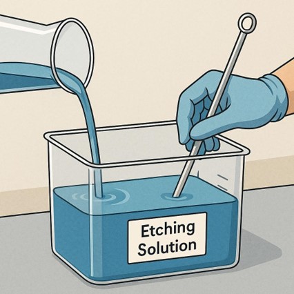
- Ferric chloride: Trusted smooth-walled copper etching solution.
- Ammonium persulphate: We recommend using a clear bath as it allows you to check the status of your etching.
- Cupric chloride: A sustainable one for a number of cycles of the copper etching process.
Step 5: Etch the Exposed Copper
During etching, the chemical solution removes only the copper areas not protected by photoresist. The goal is to create clean shapes, smooth edges, and repeatable dimensions.
For precision metal etching for copper, etch control must balance speed and accuracy. If the etch rate is too aggressive, the sidewall may widen and the final feature may exceed tolerance.
Controlled etching is valuable for photo etched copper parts with fine details. Common examples include copper electrical contacts, copper lead frame parts, copper EMI shielding, copper connectors, and precision copper components.
Step 6: Stop the Etching Reaction
Once the target depth or opening is reached, the etching reaction must stop quickly. This prevents over-etching and helps keep the final dimensions stable.
Industrial production uses controlled rinsing and cleaning instead of simple manual neutralization. The goal is to remove chemical residue without staining the copper surface.
This step is important when the parts need plating, soldering, bonding, or surface protection later. Clean copper surfaces support better finishing quality and longer service life.
Step 7: Strip the Resist
After etching, the remaining photoresist is removed from the copper surface. This reveals the final etched copper components.
The stripping step must remove the resist completely without damaging the copper surface. Any leftover residue may affect plating adhesion, electrical contact, or visual quality.
For copper shielding components and copper electrical contacts, this step also supports stable conductivity. Clean surfaces reduce the risk of poor contact in later assembly.
Step 8: Finish the Surface
Finishing depends on the final application. Some etched copper components need only cleaning, while others need plating, coating, polishing, or anti-oxidation treatment.
Copper oxidizes easily in normal storage and use. Surface protection can improve solderability, corrosion resistance, contact stability, and appearance.
For copper heat spreaders, flatness and surface cleanliness may affect thermal transfer. For copper connectors and copper busbars, plating may improve contact life and reduce surface oxidation.
Step 9: Output Paths
Industrial copper etching supports many production paths. It can produce prototypes, low-volume engineering samples, and repeatable production parts from the same digital tooling logic.
Typical applications include copper electrical contacts, copper EMI shielding, copper lead frame parts, copper connectors, copper busbars, copper heat spreaders, and copper shielding components. These parts often need fine features, clean edges, and stable conductivity.
For buyers, this makes custom copper etching useful during product development. Design changes can usually be made by updating the artwork, without building expensive stamping dies.
Step 10: Cleanup, Storage, and Disposal
The final step is inspection and controlled packaging. For B2B copper etching services, this step matters as much as the etching process itself.
Based on TMNetch production practice, etched copper components can be checked by 2D vision inspection. FAI and OQC reports can also support engineering approval and batch quality control.
When choosing a copper etching supplier, ask about tolerance control, inspection method, material traceability, surface protection, and packaging standards. These details help reduce quality risk before the parts enter assembly.
Copper Etching Solution: Key Control Factors
A copper etching solution is not just a chemical liquid. In industrial copper chemical etching, it is part of a controlled production system.
The solution affects etch rate, edge quality, undercut, surface finish, and final tolerance. For precision copper etching, stable solution control matters more than a simple chemical formula.
Key Factors to Control
A professional copper etching manufacturer usually controls these process factors:
- Etchant type: Ferric chloride and cupric chloride are common choices for chemical etching copper parts.
- Concentration: The solution strength affects etching speed and dimensional accuracy.
- Temperature: Higher temperature can increase etch rate, but it may also increase undercut.
- Acid balance: Proper acid control helps maintain stable copper removal.
- ORP: Oxidation-reduction potential shows how active the etching solution is.
- Spray pressure and flow rate: These affect how evenly the solution reaches fine features.
- Conveyor speed: Line speed controls exposure time and final etch depth.
Why Etchant Control Matters
Copper does not only etch downward. It also etches sideways under the photoresist, which is called undercut.
If undercut is not controlled, holes may become larger, narrow lines may lose width, and fine features may exceed tolerance. This is a common risk in photo etched copper parts and precision copper components.
Based on industry references for cupric chloride etching, process windows may include ORP around 540–560 mV, free acid around 1N–2N HCl, and controlled solution density. These values show why copper etching services need process monitoring, not manual guesswork.
Material Differences
Different copper alloys react differently during etching. A reliable copper etching supplier should adjust the process for each material.
Common examples include:
- Oxygen-free copper etching for high-conductivity parts
- Brass etching for connectors and decorative industrial parts
- Phosphor bronze etching for spring contacts
- Beryllium copper etching for high-strength contact parts
- Nickel silver etching for EMI and shielding components
Buyer Takeaway
For buyers, the key question is simple: can the supplier control the copper etching solution batch after batch?
Stable etchant control supports burr-free copper etching, stress-free copper etching, and repeatable etched copper components. This is important for copper electrical contacts, copper EMI shielding, copper lead frame parts, copper connectors, copper busbars, and copper heat spreaders.
Based on TMNetch production capability, copper etching can process copper foils and plates from 0.05 mm to 2.5 mm. Suitable designs can reach tolerances as tight as ±0.03 mm, depending on thickness, geometry, and drawing requirements.
Applications of Copper Etching
Copper etching is widely used when parts need high conductivity, fine patterns, and clean edges. For B2B buyers, its value is strongest in thin and flat copper parts.
Compared with stamping, copper chemical etching does not create mechanical stress. Compared with laser cutting, it avoids heat-affected zones on fine copper features.
This makes precision copper etching suitable for electrical, thermal, shielding, and micro-connection applications. It is especially useful when the design includes small holes, narrow slots, or complex outlines.
Electrical Contacts and Connectors
Copper electrical contacts need stable conductivity and accurate contact geometry. Small burrs or deformations can affect assembly pressure and electrical performance.
Burr-free copper etching helps produce clean contact edges without stamping force. This is useful for copper connectors, terminal pieces, spring contacts, and other precision copper components.
For custom copper etching, engineers can adjust finger width, slot shape, and contact layout through digital tooling. This supports prototype changes without expensive hard dies.
EMI Shielding and Copper Shielding Components
Copper EMI shielding parts help reduce electromagnetic interference in electronic devices. EMI shielding means blocking unwanted electromagnetic noise from nearby circuits or external sources.
Photo etched copper is suitable for thin shielding covers, grounding springs, shielding cans, and copper mesh. The process can form fine openings while keeping the copper surface flat.
This is useful for consumer electronics, communication devices, automotive electronics, and industrial control systems. A reliable copper etching supplier should control flatness, edge quality, and surface cleanliness.
Copper Lead Frames and Electronic Packaging Parts
A copper lead frame supports and connects a semiconductor chip inside a package. It needs stable dimensions, clean lead fingers, and good bonding surfaces.
Photochemical etching copper can create fine lead patterns without tool wear or mechanical burrs. This helps maintain repeatable lead geometry during prototype and batch production.
Copper alloy etching is also common for lead frame-related parts. Materials may include oxygen-free copper, beryllium copper, phosphor bronze, or other conductive copper alloys.
Copper Busbars and Power Distribution Parts
Copper busbars carry current inside power systems, battery packs, inverters, and industrial equipment. Their shape affects current path, contact area, and assembly reliability.
Chemical etching copper parts can support thin busbars, laminated busbar layers, tabs, and current-collecting plates. It works well when the design needs slots, holes, or complex flat profiles.
For thicker or high-current busbars, buyers should confirm thickness, current rating, and thermal rise with the supplier. Based on TMNetch production capability, copper etching can process copper foils and plates from 0.05 mm to 2.5 mm.
Copper Heat Spreaders and Thermal Components
Copper heat spreaders move heat away from hot components. Heat spreader design depends on contact area, flatness, thickness, and surface condition.
Stress-free copper etching helps produce thin copper heat spreaders without cutting stress or thermal distortion. This is useful for electronics, power modules, LED systems, and compact thermal assemblies.
For thermal parts, the buyer should define thickness, flatness, surface finish, and any plating requirement. These details affect heat transfer and downstream assembly.
Fine Copper Mesh, Screens, and Filters
Copper photo etching can create fine mesh, screens, and micro-opening parts. These parts need consistent aperture size and clean edge profiles.
Precision metal etching for copper is useful when mechanical punching may deform thin copper sheets. It can also support design changes by updating the artwork.
Common uses include copper shielding mesh, sensor screens, precision metal mesh filters, acoustic openings, and electronic protection components. For these parts, opening size, bridge width, and sheet thickness must be reviewed together.
Material-Specific Applications
Different copper alloys fit different application needs. Oxygen-free copper etching is often used when high conductivity matters.
Brass etching works well for connectors, nameplates, and decorative industrial parts. Phosphor bronze etching suits spring contacts and elastic conductive parts.
Beryllium copper etching supports high-strength contacts and spring features. Nickel silver etching is often used for shielding, corrosion-resistant parts, and decorative electronic components.
Buyer Takeaway
Copper etching services are most valuable when the part needs precision, clean edges, and design flexibility. The process is a strong option for etched copper components with fine features and repeated production needs.
When choosing a copper etching manufacturer, check material range, thickness capability, tolerance control, inspection method, and finishing options. For custom copper etching, also send the drawing, material grade, thickness, tolerance, and annual demand.
Based on TMNetch production capability, suitable copper designs can reach tolerances as tight as ±0.03 mm. Final capability still depends on copper grade, material thickness, feature size, and part geometry.
TMNetch Copper Etching Capabilities
TMNetch provides copper etching services for electronics, EMI shielding, thermal management, and industrial components. We focus on precision copper etching for parts that need clean edges, stable dimensions, and repeatable quality.
Based on TMNetch production data, we can process copper foils and plates from 0.05 mm to 2.5 mm, with part sizes up to 1500 × 600 mm. For suitable designs, our copper photo etching process can reach tolerances as tight as ±0.03 mm.
We support single-sided, double-sided, and multi-depth copper chemical etching. This makes custom copper etching suitable for copper electrical contacts, copper EMI shielding, copper lead frame parts, copper connectors, copper busbars, and copper heat spreaders.
TMNetch also supports copper alloy etching, including brass etching, phosphor bronze etching, nickel silver etching, and oxygen-free copper etching. Different materials require different process settings to control undercut, surface quality, and dimensional accuracy.
With automated etching lines and inspection support, TMNetch helps buyers move from prototype review to stable production. If you need a copper etching manufacturer for custom parts, send your drawing, material grade, thickness, tolerance, surface finish, and quantity for technical review.
FAQs on Copper Etching
Q1. What is the safest solution for copper etching?
Ferric chloride is perhaps the most safe copper etching solution that can be handled easily and produces reliable results. Safety precautions must be taken, such as the use of gloves, goggles, and cheap home shutter heating for ventilation.
Q2. How long does copper etching take?
Copper etching times will vary based on the strength of the solution, agitation, and temp. Generally, a shallow etch will be only 5–10 minutes, but deep bites need 20 minutes or more for fine detail copper plate etching.
Q3. Is copper etching okay to use on circuit boards?
Yes, making circuit boards using a copper etching process is common. Engineers create precise path ways with this technique by masking areas they do not want to be etched away and submerging the PCB into a copper etching solution.
Q4.What chemical is used to etch copper?
Copper is commonly etched with ferric chloride or cupric chloride. Some industrial copper etching processes may also use alkaline etchants.
For precision copper etching, the supplier must control concentration, temperature, ORP, spray pressure, and line speed. These factors affect etch rate, undercut, edge quality, and final tolerance.
Conclusion
Copper etching is valuable when copper parts need fine features, clean edges, and stable repeatability. For buyers, copper chemical etching is often a practical choice for etched copper components such as electrical contacts, EMI shielding parts, lead frames, connectors, busbars, and heat spreaders.
If your project needs custom copper etching, choose a copper etching supplier that can review material grade, thickness, tolerance, finishing, and inspection requirements before production. TMNetch supports precision copper etching from prototype review to volume manufacturing.