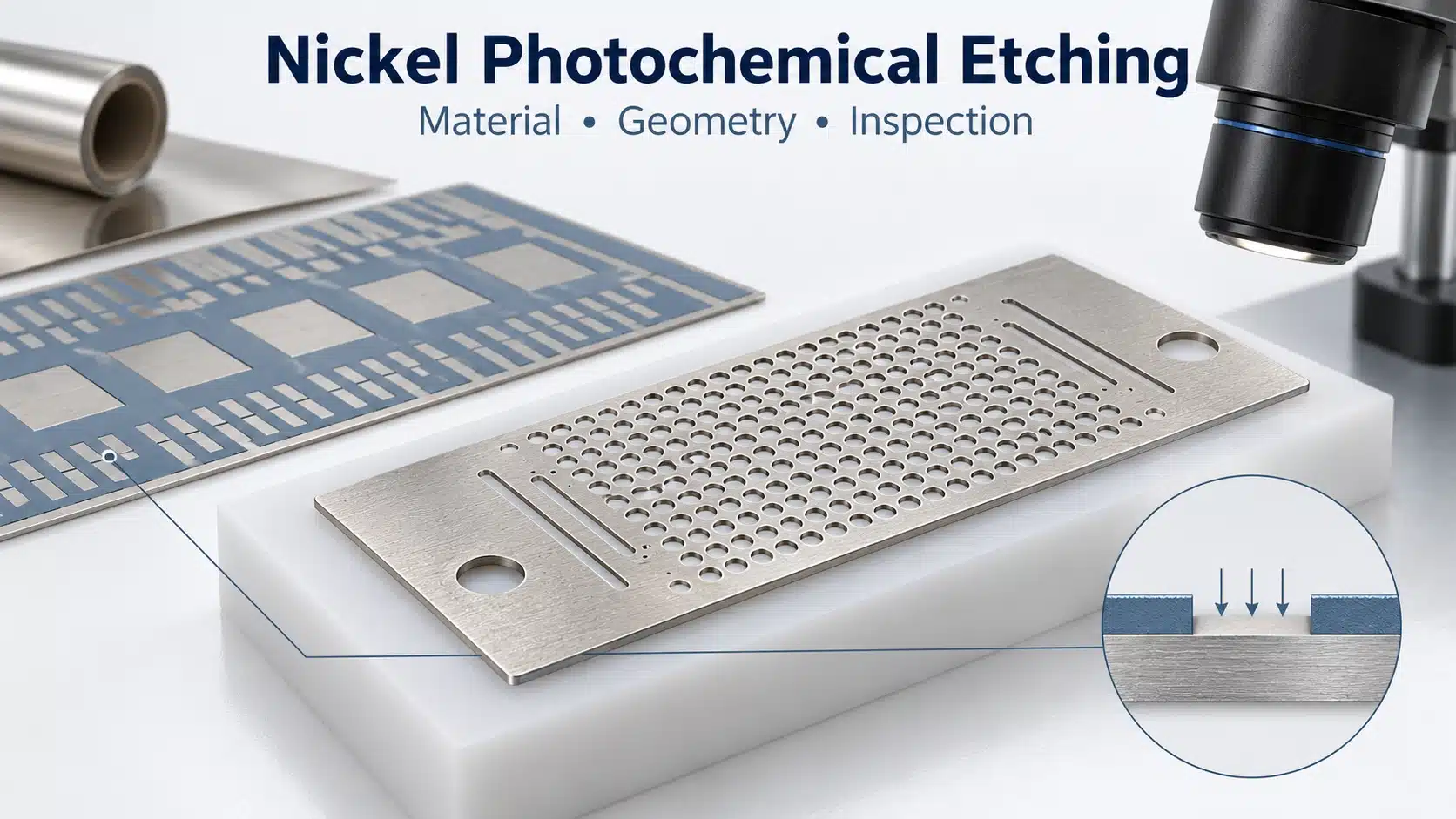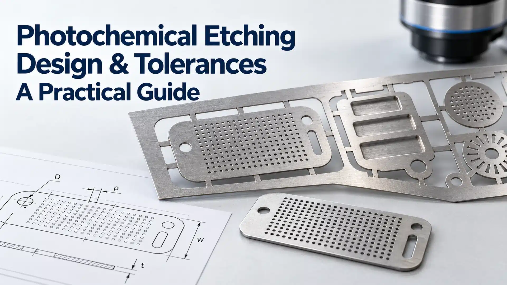

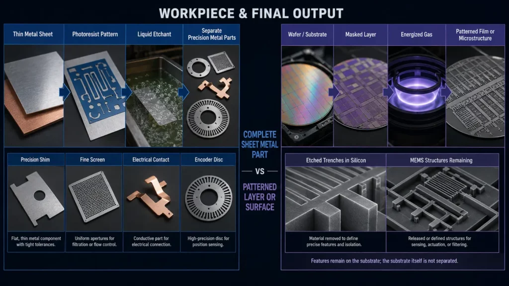
Chemical etching and plasma etching usually solve different manufacturing problems. Chemical etching uses liquid etchants and photoresist to manufacture thin, flat metal parts. Plasma etching uses energized gases to remove thin layers from wafers, films and other substrates.
Choose chemical etching for burr-free sheet metal components, complex two-dimensional patterns and flexible digital tooling. Choose plasma etching when the project needs controlled thin-film removal, directional microfeatures or surface activation.
Neither process is universally better. The right choice depends on the material, feature scale, part geometry, required profile, production volume and final application.
Key Takeaways
- Chemical etching is mainly used to manufacture thin, flat precision metal parts.
- Plasma etching is mainly used for wafers, thin films, MEMS and microelectronic structures.
- Chemical etching relies on liquid chemical reactions.
- Plasma etching may use chemical reactions, physical ion bombardment or both.
- Chemical etching can process many features across one metal sheet.
- Plasma etching can provide stronger directional control at a much smaller feature scale.
- Both processes require proper chemical, gas, waste and safety controls.
- Cost cannot be compared fairly without defining the workpiece, feature size and production requirements.
Chemical Etching vs Plasma Etching at a Glance
| Factor | Chemical etching | Plasma etching |
|---|---|---|
| Primary process | Wet chemical removal | Dry removal using energized gases |
| Typical workpiece | Thin metal sheet and foil | Wafers, substrates and thin films |
| Removal mechanism | Chemical dissolution | Chemical reaction, physical bombardment or both |
| Process environment | Etching line, spray system or chemical bath | Low-pressure or controlled plasma chamber |
| Typical geometry | Flat metal parts and through-features | Patterned films, trenches and surface layers |
| Directionality | Often more isotropic | Can be controlled for greater anisotropy |
| Main design concern | Undercut and thickness-related feature limits | Selectivity, mask erosion, ion damage and profile control |
| Tooling | Digital artwork and photo tooling | Masks, chamber recipes and process controls |
| Production approach | Multiple parts and features processed across a sheet | Wafer, substrate or chamber-based processing |
| Typical applications | Shims, filters, grilles, contacts, shields and encoder discs | Semiconductors, MEMS, optics and thin-film devices |
| Main waste stream | Spent liquid chemicals and dissolved metals | Process gases, reaction products and chamber residues |
| Typical equipment | Photoresist, imaging and etchant systems | Vacuum chamber, gas delivery, RF power and exhaust systems |
This table provides a general comparison. Actual results depend on the material, equipment and process recipe.
What Is Chemical Etching?
Chemical etching is a subtractive manufacturing process that removes selected areas from a metal sheet through a controlled chemical reaction. It is also called photochemical etching, photo etching or photochemical machining.
The process uses a photoresist to protect the metal that must remain. The exposed areas react with the etchant and dissolve. After the remaining photoresist is removed, the required metal components remain on the sheet.
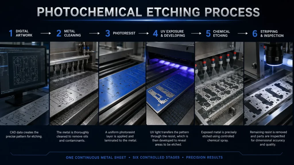
How the Chemical Etching Process Works
A typical photochemical etching process includes the following stages:
- Prepare the design: The component pattern is converted into digital tooling.
- Clean the metal: Oils, oxides and surface contaminants are removed.
- Apply photoresist: A light-sensitive resist is laminated onto the metal.
- Expose and develop: UV exposure transfers the design and opens the areas that must be etched.
- Etch the metal: A controlled etchant removes the exposed material.
- Strip and inspect: The remaining resist is removed before the parts are cleaned and checked.
Because the tooling comes from digital design data, engineers can revise a component without producing a new hard stamping die.
Multiple components, holes and slots can also be processed across the same sheet. This makes the process suitable for feature-dense metal parts.
Learn more about the chemical etching process, applications and benefits.
Common Chemical Etching Applications
Photochemical etching is commonly considered for:
- EMI and RFI shielding components
- Electrical contacts and lead frames
- Precision filters and screens
- Speaker and microphone grilles
- Shims, spacers and washers
- Encoder and code discs
- Fine metal meshes
- Flat springs
- Fuel-cell and battery components
- Medical and diagnostic components
- Decorative and functional metal panels
The material, thickness, feature dimensions and tolerance requirements must still be reviewed for each project.
What Is Plasma Etching?
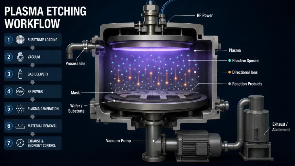
Plasma etching is a dry material-removal process that uses an energized gas. Plasma contains ions, electrons, neutral particles and chemically reactive species.
The process normally takes place in a controlled chamber. A gas enters the chamber and receives energy from a radio-frequency or other power source. This energy creates the plasma.
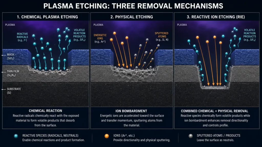
The plasma then interacts with exposed areas of the substrate. Material may be removed through:
- A chemical reaction with reactive species
- Physical bombardment by energetic ions
- A combination of chemical and physical mechanisms
Lam Research explains that plasma dry etching uses reactive radicals and ions. The ions can also provide the directionality needed to form controlled structures on semiconductor wafers. Lam Research
How the Plasma Etching Process Works
A general plasma etching process includes these stages:
- Place the substrate in the process chamber.
- Reduce the chamber pressure when the process requires a vacuum.
- Introduce the selected process gas.
- Apply energy to generate the plasma.
- Expose the unprotected substrate areas to ions and reactive species.
- Form and remove the reaction products.
- Monitor the endpoint and process conditions.
- Vent the chamber and inspect the substrate.
The exact equipment and recipe depend on the substrate, masking material, required depth and sidewall profile.
Common Plasma Etching Gases
Plasma etching may use gases based on:
- Oxygen
- Argon
- Chlorine
- Fluorine
- Fluorocarbons
- Other application-specific chemistries
These gases do not perform the same function.
Argon is often associated with physical sputtering or ion bombardment. Oxygen plasma may remove organic materials or activate surfaces. Chlorine- and fluorine-based chemistries can react with selected semiconductor, dielectric or metal layers.
The gas must be matched to the target material and required selectivity. Plasma etching does not remove every material in the same way.
Common Plasma Etching Applications
Plasma etching is widely associated with:
- Semiconductor wafer fabrication
- Integrated circuits
- Microelectromechanical systems
- Thin-film patterning
- Sensors
- Photonic and optical devices
- Microfluidic structures
- Surface cleaning and activation
- Photoresist removal
- Research microfabrication
These are different from the thin sheet metal applications normally associated with photochemical etching.
Is Plasma Etching the Same as Physical Etching?
Plasma etching and physical etching are related, but the terms are not interchangeable.
Physical etching describes a material-removal mechanism. Energetic ions strike the surface and transfer enough momentum to eject atoms. Sputter etching, ion milling and some forms of ion beam etching mainly use this mechanism.
Plasma etching describes a broader process category. It can rely on:
- Physical ion bombardment
- Reactions between active species and the surface
- A combination of physical and chemical removal
Reactive ion etching, commonly called RIE, combines the two mechanisms. Directional ions strike the surface while reactive species form removable by-products.
OSHA describes sputter etching and ion beam milling as physical processes, while RIE combines chemical and physical effects. OSHA semiconductor fabrication guidance
Oxford Instruments also distinguishes inert ion beam milling from processes that add reactive gases to improve material selectivity and etch rate. Oxford Instruments
A separate physical etching guide can explore ion milling, sputter etching and related dry-etching methods in more detail.
Chemical Etching vs Plasma Etching: Key Differences
1. Material-Removal Mechanism
Chemical etching removes material through a reaction between a liquid etchant and the exposed metal.
Plasma etching uses gases instead of a liquid bath. Depending on the process, the removal may come from reactive species, energetic ions or both.
This difference affects the equipment, scale, process control and type of component each method can produce.
2. Part and Feature Scale
Chemical etching normally manufactures complete parts from metal sheet or foil. It can produce outside profiles, holes, slots and repeated openings.
Plasma etching more often removes thin surface layers from a wafer or substrate. It is central to microelectronics because it can pattern features and layers at a much smaller scale.
This difference is important. A thin-film etch depth should not be compared directly with the total thickness of a sheet metal component.
3. Materials
Chemical etching can process many metals when a suitable etchant and process are available. Examples include selected grades and forms of:
- Stainless steel
- Copper
- Brass
- Phosphor bronze
- Nickel alloys
- Titanium
- Aluminum
Different alloys respond differently to an etchant. Surface condition, temper, thickness and chemistry can affect the result.
See the photochemical etching materials guide for a broader material overview.
Plasma etching can process many semiconductor materials, dielectric films, polymers, metals and optical materials. However, it is not correct to say that every material can be etched with the same plasma process.
The supplier must match the process gas, mask, power, pressure and chamber configuration to the substrate.
4. Directionality and Undercut
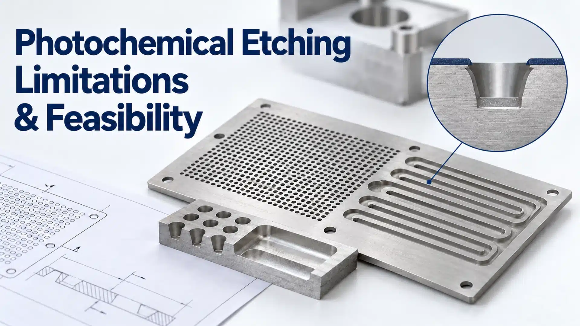
Photochemical etching usually removes metal downward and sideways. The sideways removal beneath the photoresist is called undercut.
Undercut affects:
- Minimum hole size
- Minimum slot width
- Minimum web width
- Edge profile
- Dimensional tolerance
These limits become more important as the metal becomes thicker or the features become smaller.
Plasma processes can offer more directional removal. Energetic ions can travel toward the substrate in a controlled direction, which helps create more vertical sidewalls.
However, plasma etching does not automatically eliminate all profile errors. Results still depend on:
- Ion energy
- Gas chemistry
- Chamber pressure
- Mask selectivity
- Redeposition
- Substrate temperature
- Feature aspect ratio
For chemical etching design factors, see the photochemical etching tolerances and limits guide.
5. Precision
It is misleading to state that one method is always more precise.
Chemical etching can provide repeatable dimensions for thin, flat metal parts. Its practical tolerance depends on material thickness, alloy, feature geometry and process control.
Plasma etching can achieve very small patterned features in semiconductor and microfabrication applications. It can also provide controlled sidewall profiles and thin-film removal.
The two types of precision are not directly comparable. One process manufactures sheet metal components, while the other often patterns films and structures on a substrate.
6. Edge and Surface Effects
Chemical etching does not use a cutting tool. It therefore avoids the conventional mechanical burrs associated with punching, milling or some cutting processes.
It also avoids the concentrated heat source used in laser cutting. This is useful for thin parts that are sensitive to cutting force or thermal distortion.
Plasma etching does not create a mechanical cutting burr either. However, energetic ion bombardment can affect sensitive substrate surfaces. Some processes may also create redeposition, mask erosion or surface damage.
The acceptable surface condition must be defined for the final application.
7. Production Speed and Throughput
Neither process is always faster.
Chemical etching can arrange many components on a single metal sheet. Their exposed features are processed during the same etching stage. This can be efficient for parts with many holes, slots or repeated patterns.
Plasma etching may process complete wafers or substrate batches. Its throughput depends on chamber size, load method, target depth, material, gas chemistry and recipe time.
A meaningful comparison should use:
- Parts or wafers per batch
- Required material-removal depth
- Number of features
- Setup time
- Inspection requirements
- Expected production volume
Statements such as “plasma etching is always faster” or “plasma processes only one component at a time” are not reliable.
8. Tooling and Design Changes
Chemical etching uses digital artwork and photo tooling. Changing the part design often requires an artwork update rather than a new hard die.
This can support:
- Engineering prototypes
- Design iterations
- Multiple part variants
- Low-to-medium production volumes
- Bridge production
- Products with changing requirements
Plasma etching also depends on digital pattern data and masking processes. However, each process requires a controlled chamber recipe matched to the substrate and target layer.
Changing the material or feature profile may require recipe development, mask changes and process validation.
9. Equipment and Cost
Chemical etching normally uses:
- Cleaning systems
- Photoresist coating equipment
- UV imaging
- Development equipment
- Etchant delivery and control systems
- Chemical recovery or treatment systems
- Inspection equipment
Plasma etching normally requires:
- A controlled process chamber
- Vacuum equipment
- RF or other power systems
- Gas delivery and monitoring
- Chamber cooling or temperature control
- Exhaust and abatement equipment
- Endpoint monitoring
- Chamber maintenance
Plasma equipment can require higher capital investment and more specialized process control. Chemical etching still carries costs for chemicals, wastewater treatment, process monitoring and safe operation.
Unit cost depends on more than the equipment price. Buyers should also evaluate:
- Material utilization
- Tooling
- Batch capacity
- Recipe development
- Inspection
- Waste treatment
- Maintenance
- Design changes
- Production volume
- Required secondary operations
Chemical etching may be more economical for complex sheet metal parts. Plasma etching may be justified when the required feature scale or thin-film profile cannot be achieved through wet sheet-metal etching.
10. Environmental and Safety Considerations
Chemical etching creates liquid waste that may contain spent etchant, dissolved metals and process chemicals. A manufacturer must control storage, ventilation, treatment and disposal.
Plasma etching produces less liquid waste, but this does not make it automatically harmless.
Dry etching may use fluorinated, chlorinated or other reactive gases. OSHA identifies reactive gases, reaction residues and RF energy as potential dry-etching hazards that require ventilation, monitoring and suitable controls. OSHA
Some fluorinated gases used in semiconductor manufacturing also have high global warming potential. The U.S. EPA lists compounds such as CF₄, C₂F₆, NF₃ and SF₆ and explains the importance of gas utilization and abatement. U.S. EPA
A responsible environmental comparison should therefore consider:
- Chemical consumption
- Liquid waste
- Gas consumption
- Energy use
- Unreacted emissions
- Exhaust abatement
- Worker exposure controls
- Recovery and recycling
- Local regulations
Neither process should be described as environmentally safe without examining the actual facility and controls.
Plasma Surface Treatment vs Material-Removal Etching
Not every plasma process is used to create a part or deep pattern.
Plasma treatment may also clean, activate or modify the outer surface without removing enough material to form the complete component geometry.
Plasma Cleaning
Plasma cleaning can remove selected organic contamination and surface residues. The goal is to prepare the surface for another manufacturing stage.
Plasma Activation
Plasma activation changes the surface so that liquids, coatings or adhesives can wet it more effectively. Higher surface energy can improve wettability and support bonding, printing, sealing or coating.
Plasmatreat describes plasma treatment as a way to clean and activate surfaces while improving wettability and adhesion. Plasmatreat
Plasma Etching
Plasma etching removes material from selected surface areas. It may also roughen or modify the surface, depending on the process.
Chemical Etching
Photochemical etching removes enough metal to create the geometry of a thin sheet metal component. It is used for profiles, holes, slots and other designed features.
This distinction is important when the next step is plating or coating.
If the goal is to improve plating adhesion, the project may require cleaning, oxide removal or surface activation rather than complete material-removal etching. The process should be validated using the actual base material, surface condition, plating system and performance requirements.
Surface energy alone does not guarantee a successful plated layer. Cleanliness, oxide condition, roughness, chemistry and time between treatment and plating can also affect the result.
Advantages of Chemical Etching
Chemical etching offers several advantages for suitable metal components.
Burr-Free Metal Parts
Chemical removal does not create the sheared burr associated with punching or mechanical cutting.
This can reduce deburring requirements and protect sensitive mating surfaces.
Low Mechanical Stress
The process does not push a cutting tool or punch through the component. Thin parts are therefore less exposed to machining force or difficult clamping.
No Concentrated Cutting Heat
Chemical etching is not a thermal cutting process. It avoids laser-style heat-affected zones and focused heat distortion.
Flexible Digital Tooling
Engineers can update the artwork when a design changes. This is useful during development and before a design becomes stable.
Complex Two-Dimensional Features
Holes, slots, openings and outside profiles can be included in the same design. Feature complexity does not require a separate mechanical cutting tool for every shape.
Multiple Designs on One Sheet
Different components may share a production sheet when their material, thickness and process requirements are compatible.
Suitable for Thin and Delicate Parts
Thin components can be difficult to machine or clamp. Chemical etching removes material without direct cutting pressure.
Chemical etching still has practical limits. Material thickness, undercut and minimum feature dimensions must be considered. Read more about the limitations of photochemical etching.
Advantages of Plasma Etching
Plasma etching offers different advantages for thin-film and substrate applications.
Controlled Directionality
Ion movement can help produce directional removal and controlled sidewall profiles.
Small Feature Scale
Plasma processes are central to semiconductor and MEMS manufacturing, where features are much smaller than conventional sheet metal parts.
Thin-Film Selectivity
A suitable chemistry can remove a target film while limiting removal from neighboring materials. The achievable selectivity depends on the full process.
Dry Processing
The material-removal stage does not require immersing the substrate in a liquid etchant.
Surface Modification
Plasma can support cleaning, activation, oxide removal and controlled surface modification in addition to material removal.
Advanced Profile Control
Plasma parameters can be adjusted to control etch rate, profile and directionality. This is important for microelectronic and photonic structures.
These benefits come with higher equipment complexity and strict process-control requirements.
When Is Chemical Etching the Better Choice?
Chemical etching is often the better fit when the project requires:
- A complete part made from thin metal sheet or foil
- Burr-free edges
- Low mechanical stress
- No concentrated cutting heat
- Many holes, slots or repeated openings
- Complex two-dimensional geometry
- Low-cost design changes
- Prototype and production flexibility
- Several part variants
- Components such as filters, shims, grilles, shields or contacts
A chemical etching supplier should review the drawing before confirming feasibility.
When Is Plasma Etching the Better Choice?
Plasma etching is often the better fit when the project requires:
- Patterning on a wafer or substrate
- Removal of a thin deposited layer
- Semiconductor or MEMS fabrication
- Directional microfeatures
- Controlled sidewall profiles
- High-aspect-ratio structures
- Surface activation
- Plasma cleaning
- Processing of materials that require a specialized dry-etch recipe
- Integration with other thin-film manufacturing stages
Plasma etching may be technically capable but commercially unnecessary for a conventional thin sheet metal part.
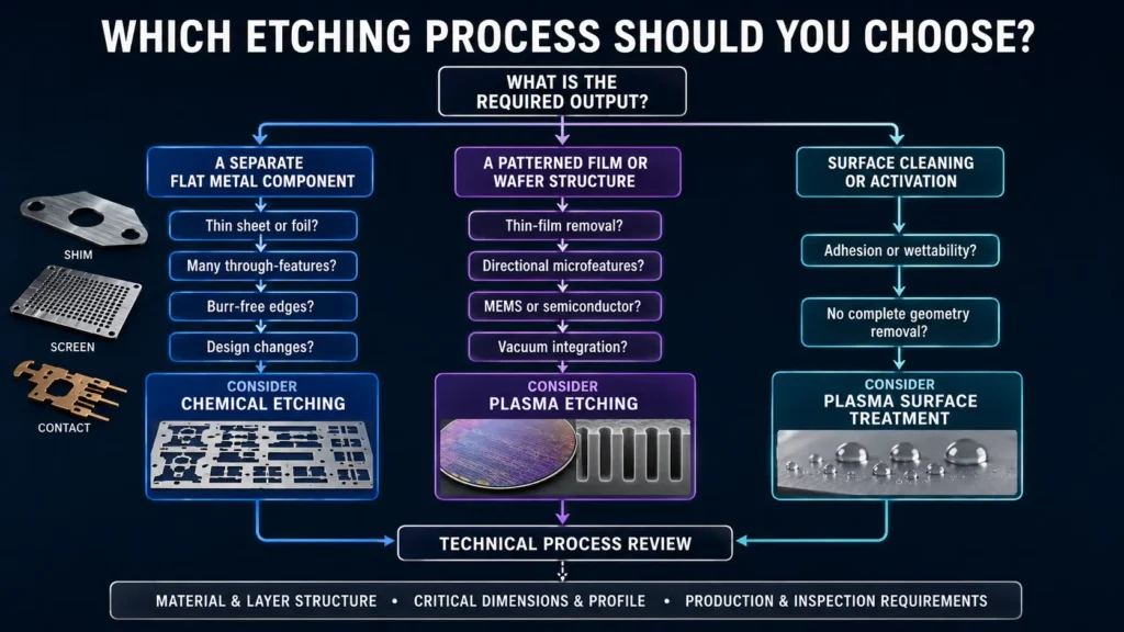
Which Etching Process Should You Choose?
Start by defining the manufacturing task.
Choose Chemical Etching If:
- The output is a separate flat metal component.
- The material is thin sheet or foil.
- Burr-free edges are important.
- The design contains many through-features.
- The part may change during development.
- Digital tooling provides a cost advantage.
Choose Plasma Etching If:
- The output remains part of a wafer or substrate.
- The target is a thin film or surface layer.
- Directional profile control is important.
- The application belongs to semiconductor, MEMS or microfabrication.
- Surface cleaning or activation is the main goal.
- The process must integrate with vacuum-based fabrication.
Ask for a Technical Review If:
- The smallest feature is close to the material thickness.
- The project combines through-features and partial-depth features.
- Surface condition affects plating or bonding.
- The material has several layers.
- The application has strict contamination limits.
- You are comparing costs across very different manufacturing methods.
Information Needed for Process Selection
Provide the following information when comparing chemical and plasma etching:
- Material name and grade
- Sheet thickness or film thickness
- Overall dimensions
- Smallest hole, slot or line
- Required depth
- Critical tolerances
- Required sidewall profile
- Surface finish
- Burr requirements
- Thermal and mechanical sensitivity
- Surface activation or adhesion requirements
- Prototype quantity
- Expected production volume
- Inspection method
- Secondary coating, plating or forming
- Drawing or pattern file
For a photochemical etching RFQ, a dimensioned drawing and material specification are especially important.
Can Chemical and Plasma Etching Be Combined?
Yes, wet chemical and plasma processes can appear in the same manufacturing workflow.
For example, a semiconductor or microfabrication process may use wet cleaning or selective wet etching at one stage and plasma etching at another. Each process handles a different material, layer or profile requirement.
However, this does not mean every metal part should undergo both processes.
For a conventional precision sheet metal component, adding plasma etching may increase cost without improving the required geometry. For a multilayer wafer or advanced device, using both wet and dry processes may be necessary.
The complete process flow should be designed around the final device, not around a general preference for one etching method.
Frequently Asked Questions
Is Plasma Etching Better Than Chemical Etching?
Not in every application.
Plasma etching is better suited to many thin-film, semiconductor and directional microfeature requirements. Chemical etching is often better for complete thin sheet metal parts with complex two-dimensional geometry.
Is Plasma Etching a Physical or Chemical Process?
It can be physical, chemical or a combination of both.
Ion milling mainly uses physical bombardment. Chemical plasma etching relies more on reactive species. Reactive ion etching combines ion bombardment with chemical reactions.
Is Plasma Etching the Same as Dry Etching?
Plasma etching is a major form of dry etching, but the terms are not always identical.
Dry etching is a broad category that includes plasma-based chemical etching, sputter etching, ion milling and reactive ion etching.
Does Plasma Etching Use Chemicals?
Plasma etching does not normally use a liquid etchant, but it may use chemically reactive gases.
The gas chemistry is a central part of many plasma etching processes.
Which Process Is More Cost-Effective?
Chemical etching is often more cost-effective for thin, flat metal components, especially when the design is complex or likely to change.
Plasma etching may be cost-effective when its feature scale, directionality or thin-film control is essential. Comparing only equipment prices does not provide a reliable answer.
Can Plasma Treatment Improve Adhesion Before Plating?
Plasma treatment can clean, activate or modify a surface and may improve wettability. This can support some coating or bonding processes.
Plating performance also depends on oxides, contamination, base material, pretreatment chemistry and the plating system. The complete process must be validated.
Which Process Is Better for Mass Production?
The answer depends on the product.
Chemical etching can process many sheet metal parts on one panel. Plasma tools may process wafers or substrate batches. Throughput must be measured using the required feature depth, batch capacity and inspection standards.
Can Chemical Etching Produce Semiconductor Features?
Wet chemical etching is used in some semiconductor processes, but industrial photochemical etching of metal sheet serves a different scale and manufacturing purpose.
Do not assume that the capabilities of semiconductor wet etching apply directly to precision sheet metal components.
Conclusion
Chemical etching and plasma etching are both material-removal processes, but they usually serve different products.
Chemical etching uses liquid chemistry and digital photo tooling to manufacture thin, flat metal components. It is suitable for feature-dense designs, burr-free edges and projects that may require design changes.
Plasma etching uses energized gases to remove or modify thin surface layers. It is widely used in semiconductor, MEMS, optical and thin-film applications that need controlled profiles or surface properties.
The first question should not be “Which process is more advanced?” It should be:
Are you manufacturing a separate sheet metal component, patterning a thin film, or modifying a surface?
If your project involves a precision metal part made from sheet or foil, contact TMNetch and submit your drawing for a chemical etching feasibility review.