
Copper etching PCB is the process of removing unwanted copper from a copper-clad board to form circuit traces, pads, and conductive patterns. A similar selective-removal principle is also used in precision copper etching, where protected copper remains and exposed copper is removed to create standalone copper components. For buyers, the key difference is the final product: a circuit pattern on a board or a precision copper part for an industrial assembly.
What Is Copper Etching in PCB Manufacturing?
In PCB manufacturing, copper etching removes copper that is not needed for the circuit. The areas that must remain are protected by a resist. The exposed copper is removed by an etchant, leaving the required copper traces and pads.
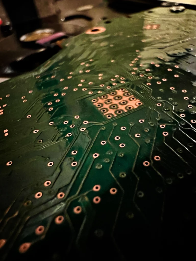
A printed circuit board uses conductive copper features to connect electronic components. Chemical etching can divide copper foil into circuit traces, pads, and conductive planes.
How Copper Layers Become Circuit Traces
Most PCB copper etching starts with a copper-clad board. The circuit image is transferred onto the copper surface. The protected copper becomes the final conductive path.
The etching step removes the unprotected copper. This is why copper etching quality affects line width, spacing, and circuit reliability.
Why Copper Etching Matters for PCB Performance
PCB copper etching must keep the copper traces close to the design. If the etching process removes too much copper, traces may become too narrow. If it removes too little copper, unwanted copper may remain between conductors.
For engineers, this can affect short-circuit risk, open-circuit risk, impedance, and signal performance. This is why the PCB etching process must be controlled carefully.
Basic PCB Copper Etching Process
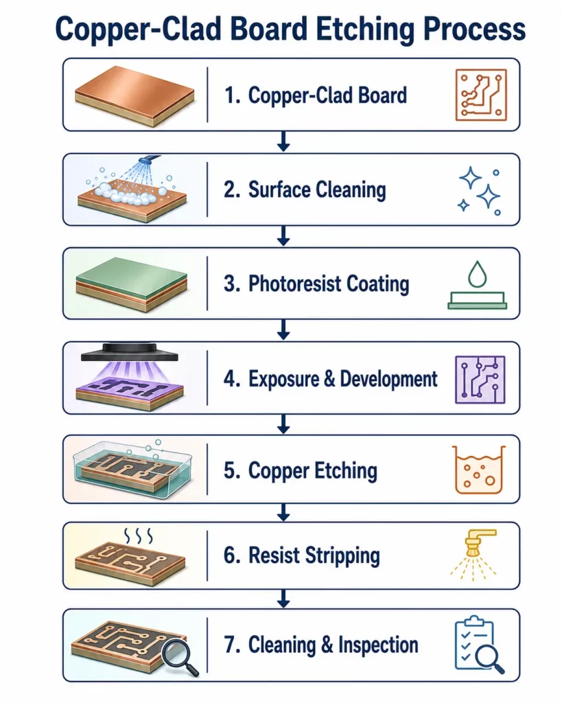
A typical PCB copper etching process follows four main steps.
Step 1: Prepare the Copper-Clad Board
The copper surface must be clean before imaging. Oils, oxides, dust, and residue can affect resist adhesion. Poor surface preparation may lead to uneven etching or poor pattern transfer.
Step 2: Apply and Image the Resist
A photoresist or etch resist protects the copper areas that must remain. The circuit pattern is transferred to the resist layer through exposure and development.
The resist acts as a mask. It tells the etchant which copper areas should stay and which areas should be removed.
Step 3: Remove Exposed Copper With Etchant
In subtractive PCB manufacturing, unwanted copper is removed from a copper-clad board, leaving only the desired copper pattern. Commercial etching often uses spray etching, where nozzle pattern, flow rate, temperature, and etchant composition affect control.
In our production experience, copper etching quality starts before the etchant touches the metal. The copper surface must be clean, the resist pattern must be stable, and the exposed copper areas must match the drawing. These steps affect whether the final copper features are accurate, clean, and repeatable.
Step 4: Strip Resist, Clean, and Inspect
After etching, the resist is removed. The board or part is cleaned and inspected. For PCB work, this helps confirm that the copper traces are free of opens (no open circuits), clean, and close to the design.
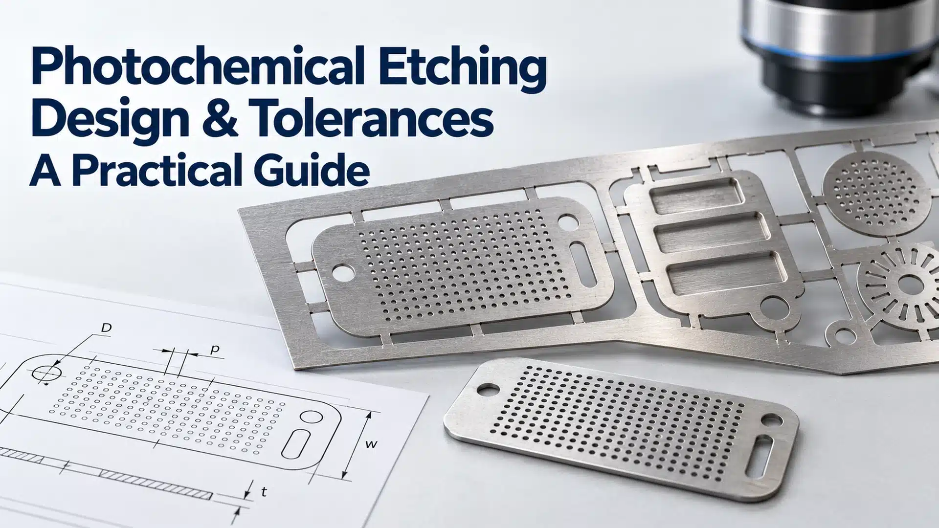
For precision copper chemical etching, inspection also checks part geometry, edge quality, hole size, flatness, and surface condition.
Common PCB Etching Methods
PCB etching can use several methods. Wet chemical etching is common in PCB production, while dry, plasma, and laser methods may be used for more specialized requirements.
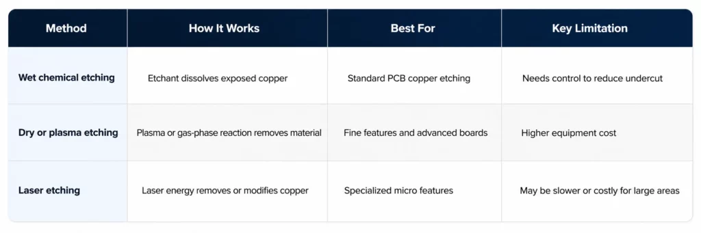
Wet chemical etching remains important because it can process copper patterns efficiently. But it still requires process control. Etchant concentration, temperature, spray pressure, dwell time, and resist quality can all affect the final copper geometry.
Common PCB Copper Etching Problems
PCB copper etching problems usually come from poor process control, weak resist, incorrect etch time, or surface contamination. The most common issues include over-etching, under-etching, undercut, and residue.
Over-Etching
Over-etching means the process removes more copper than intended. In PCB manufacturing, this can narrow copper traces and weaken the circuit path.
For fine-pitch designs, small line width changes can matter. Buyers should review how the supplier controls etch time and inspection.
Under-Etching
Under-etching means some unwanted copper remains. This can create bridges between conductors. In severe cases, it can increase short-circuit risk.
Under-etching can happen when the etchant is weak, process time is too short, or the copper surface is not prepared well.
Undercut and Line Width Loss
Undercut happens when the etchant attacks copper under the resist edge. PCB manufacturing references note that undercut can reduce conductor width and may cause open circuits, so etch time must be controlled.
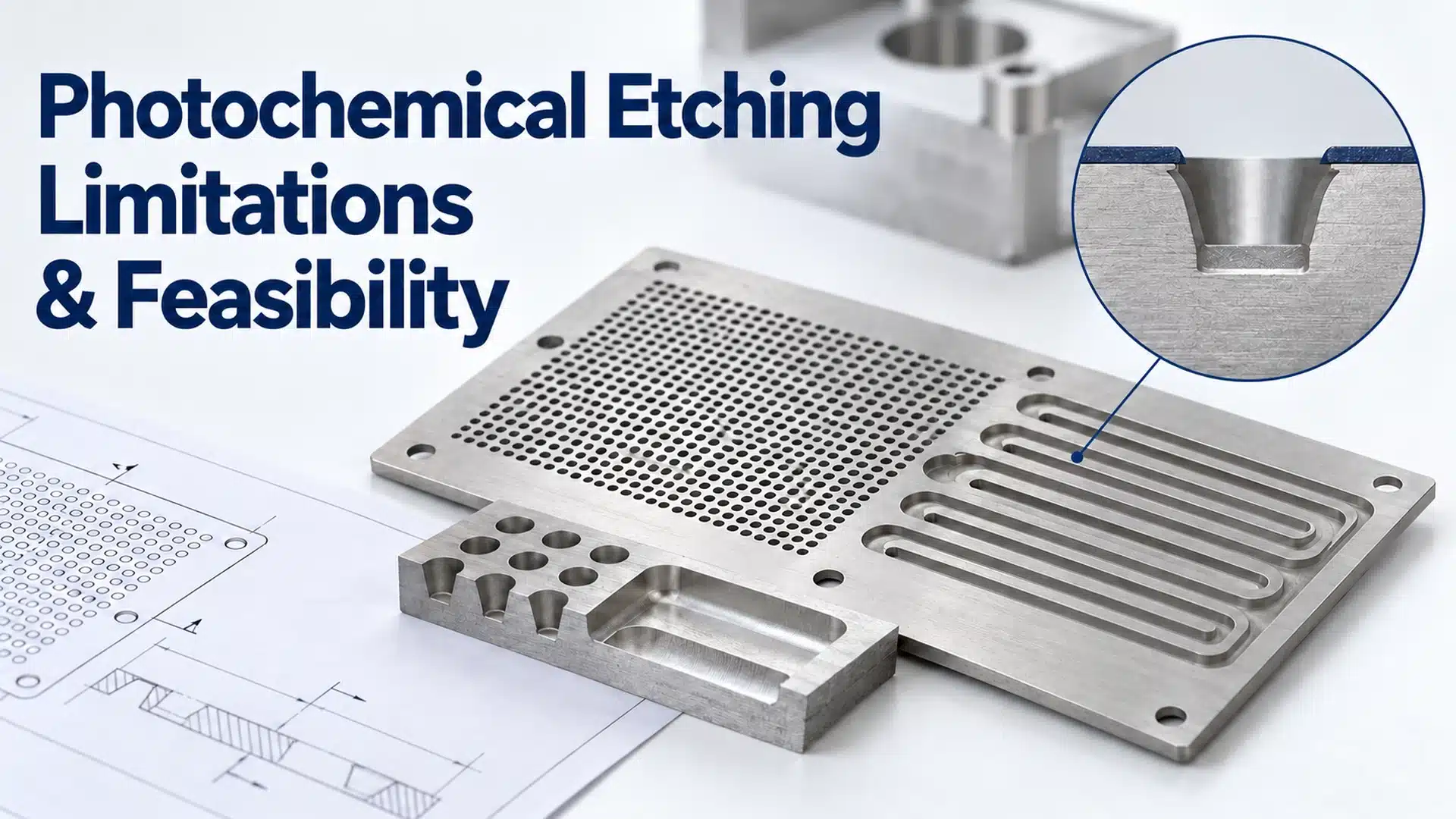
This issue is not limited to PCB production. In precision copper etching, undercut also affects slots, holes, ribs, and edge profiles.
Residue and Surface Cleanliness
Residue can affect soldering, plating, bonding, coating, or electrical contact. For copper parts, surface cleanliness is especially important when the part needs conductivity, thermal transfer, or later surface treatment.
This is why cleaning and inspection should be part of the copper etching process, not an afterthought.
From PCB Copper Etching to Precision Copper Chemical Etching
PCB copper etching and precision copper chemical etching share the same basic idea: protect selected copper and remove exposed copper.
The output is different. PCB copper etching forms conductive traces on a substrate. Precision copper chemical etching uses a similar selective-removal principle, but the output is usually a standalone copper component.
Research on direct bonded copper substrates also shows that copper patterns can be produced through masked etching routes, which supports the broader idea that selective copper removal can form functional conductive structures beyond standard PCB traces.
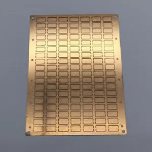
The Shared Principle: Protect Selected Copper, Remove Exposed Copper
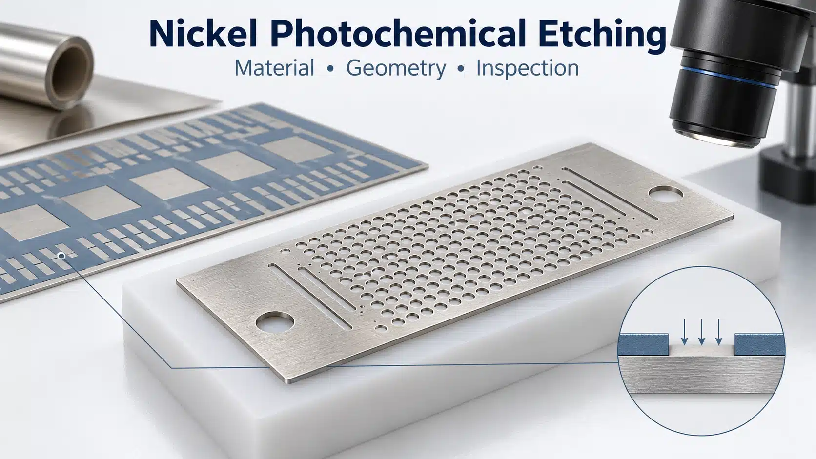
Photochemical machining uses photoresist and etchants to fabricate sheet metal components. It can produce complex parts with fine details and is often used as an alternative to stamping, punching, laser cutting, waterjet cutting, or EDM for thin-gauge precision parts.
This principle makes copper chemical etching useful beyond PCB traces. It can create thin copper parts with complex outlines, fine openings, and detailed patterns.
The Output Is Different
In PCB manufacturing, the copper remains attached to a board. The goal is an electrical circuit.
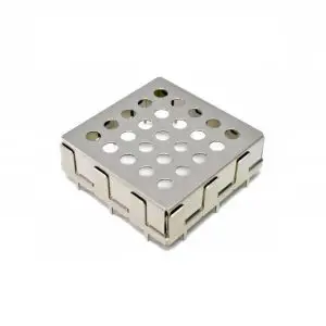
In precision copper etching, the copper part itself is the product. The goal may be a connector, contact, shield, lead frame, heat spreader, gasket, or custom copper component.
Typical Precision Copper Etched Components
Precision copper etching can support many industrial parts, including:
- Copper contacts
- Copper connectors
- EMI/RFI shielding parts
- Lead frames
- Heat spreaders
- Battery terminals
- Copper springs
- Custom copper components
TMNetch lists lead frames, heat management parts, EMI/RFI shielding, electrical components, decorative items, photovoltaic cells, and custom copper components among the precision copper etched parts it supplies.
Why Copper Etching Quality Matters in Precision Metal Manufacturing
For PCB work, copper etching quality affects circuit performance. For precision metal manufacturing, it affects part fit, assembly, conductivity, surface finish, and long-term reliability.
Edge Quality
Clean edges matter when copper parts fit into assemblies. Burrs can interfere with contact, sealing, bonding, or plating.
Chemical etching can help produce smooth, burr-free edges. TMNetch states that its copper etching process avoids mechanical stress, heat damage, and burrs, while producing smooth edges and accurate dimensions.
Dimensional Accuracy
Precision copper components often include holes, slots, contact areas, spring features, or fine profiles. These features need stable dimensions from prototype to production.
TMNetch states that its copper etching capability can achieve tolerances as tight as ±0.03 mm, depending on design and requirements.
Surface Cleanliness
Copper parts are often used for electrical or thermal functions. Surface residue can affect plating, conductivity, soldering, bonding, and coating.
A strong copper etching process should include cleaning and inspection after etching. TMNetch states that its process includes cleaning and 2D vision inspection, with FAI and OQC reports.
Prototype-to-Production Repeatability
Many OEM and ODM projects start with small prototypes. After design approval, the same part may move into volume production.
Chemical etching can help when the geometry is complex and the design may still change. Photo tooling is more flexible than hard tooling for early design iterations.
When Should Buyers Consider Copper Chemical Etching?
Buyers should consider copper chemical etching when the project requires thin copper parts, complex features, clean edges, and design flexibility.
When the Part Is Thin and Complex
Copper chemical etching is well suited for thin copper sheets and copper alloy parts. It can form fine holes, slots, channels, and detailed outlines without mechanical cutting force.
TMNetch states that it can process copper from 0.05 mm foils to 2.5 mm plates, with part sizes up to 1500 mm × 600 mm.
When Burr-Free Edges Are Important
Burr-free copper parts are useful for contacts, connectors, shielding parts, lead frames, and heat management components. Clean edges can reduce assembly risk and secondary deburring.
This is one reason buyers compare copper chemical etching with stamping, punching, or mechanical cutting.
When Tooling Flexibility Matters
If the copper design may change, custom copper etching can support faster design updates than hard tooling. This is useful during prototype validation and early engineering review.
It also helps when the part has many repeated small features, because etching forms the pattern across the sheet rather than cutting each feature one by one.
When Copper Performance Matters
Copper is widely used for electrical parts because of its high conductivity. The International Annealed Copper Standard is a commercial standard for copper conductivity and is often used as a comparative reference for other metals.
For this reason, copper material selection matters. Buyers should review copper grade, thickness, temper, surface finish, conductivity, plating needs, and inspection requirements before production.
For electrical contacts, connectors, busbars, and shielding parts, buyers should also review copper grade and conductivity. Pure copper conductors are commonly specified by electrical conductivity, and some research reports pure copper conductivity values above 100% IACS for electrical conductor applications.
How TMNetch Supports Copper Etching Projects
TMNetch provides copper etching service for precision copper and copper alloy components. Its copper etching page describes the process as controlled chemical removal from copper sheets to create precise patterns, circuits, and components.
Copper Etching Service for Precision Components
Based on TMNetch copper etching capability data, the company supports copper and copper alloy parts from 0.05 mm foils to 2.5 mm plates. It can also process parts up to 1500 mm × 600 mm.
TMNetch lists single-sided, double-sided, and multi-depth etching options. These options can support designs with channels, stepped features, fine openings, and complex copper geometries.
Materials and Applications
TMNetch lists copper and copper alloy grades including C11000, C26000, C28000, C51000, C54400, C70600, C71500, and C75200. These materials support different needs for conductivity, corrosion resistance, strength, and forming behavior.
Applications include lead frames, heat management parts, EMI/RFI shielding, electrical components, photovoltaic parts, and custom components made to drawings.
Engineering Review Before Production
For buyers, the best copper etching result starts with a complete technical review. Drawings, material grade, copper thickness, tolerance, surface finish, plating needs, and inspection requirements should be reviewed together.
If your project requires copper traces, copper contacts, shielding parts, or other custom copper components, contact TMNetch to discuss your copper etching project before production.
FAQs About Copper Etching PCB and Precision Copper Etching
What is copper etching in PCB manufacturing?
Copper etching in PCB manufacturing removes unwanted copper from a copper-clad board. The remaining copper forms circuit traces, pads, and other conductive areas.
What is the purpose of copper etching in a PCB?
The purpose is to create the required electrical pattern. Etching removes exposed copper while protected copper remains as the final circuit path.
What is the difference between PCB copper etching and precision copper etching?
PCB copper etching forms conductive traces on a substrate. Precision copper etching uses a similar selective-removal process, but it usually creates standalone copper components.
What causes over-etching in PCB manufacturing?
Over-etching can happen when etch time, etchant strength, temperature, spray pressure, or resist quality is not controlled well. It can reduce copper trace width and affect circuit reliability.
Can copper etching be used for precision metal parts?
Yes. Copper chemical etching can be used for thin copper parts, copper contacts, connectors, EMI/RFI shielding, lead frames, heat spreaders, and other precision copper components.
What industries use chemically etched copper components?
Chemically etched copper components are used in electronics, automotive, medical, aerospace, energy, photovoltaic, and industrial applications. These projects often require conductivity, clean edges, complex geometry, or thin copper features.
Conclusion
Copper etching PCB work and precision copper chemical etching share the same core idea: protect the copper areas you need and remove the copper areas you do not need.
In PCB manufacturing, this forms circuit traces on a board. In precision metal manufacturing, it forms copper contacts, connectors, shielding parts, lead frames, heat spreaders, and other custom copper components.
For buyers, the right question is not only how copper etching works. The better question is whether the project needs a circuit pattern, a standalone precision copper component, or both. If your design requires thin copper geometry, clean edges, stable dimensions, or copper alloy review, TMNetch can help review your copper etching requirements before production.