
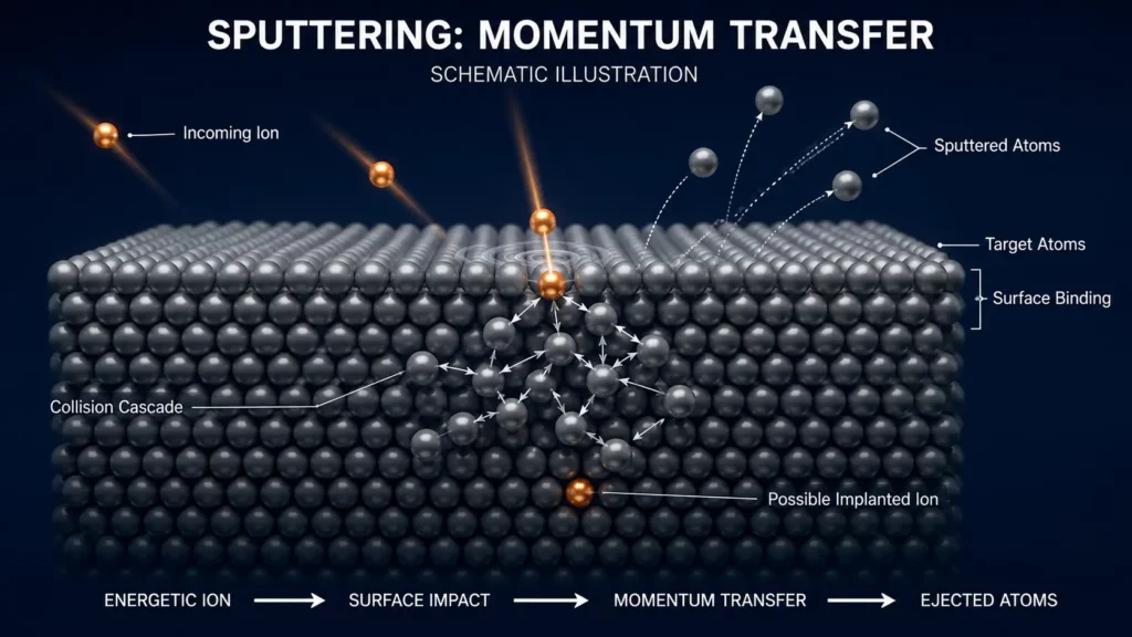
Physical etching removes material by directing energetic ions toward a surface. The ions transfer momentum to surface atoms and eject them from the material. This mechanism is called sputtering.
Physical etching is mainly used in semiconductor, thin-film, optical and materials research applications. Common methods include sputter etching, ion milling and ion beam etching.
Unlike wet chemical etching, the material-removal stage does not depend mainly on a liquid chemical reaction. Unlike purely chemical plasma etching, it can remove materials that do not easily form volatile reaction products.
However, physical etching also has limits. It can be slow, damage sensitive surfaces and provide poor selectivity between different materials.
Key Takeaways
- Physical etching removes material through ion bombardment and momentum transfer.
- It is usually a dry process performed in a vacuum or low-pressure chamber.
- Sputter etching, ion milling and inert ion beam etching are common examples.
- Physical etching is related to plasma etching, but the two terms are not identical.
- Reactive ion etching combines physical bombardment with chemical reactions.
- Physical etching can produce directional profiles and controlled sidewalls.
- Common limitations include low selectivity, surface damage, redeposition and high equipment costs.
- It is mainly used for wafers, thin films, multilayer structures and surface preparation rather than conventional sheet metal parts.
What Is Physical Etching?
Physical etching is a material-removal process in which energetic particles strike a surface and dislodge atoms.
Within semiconductor and thin-film fabrication, these particles are usually positively charged ions. Argon is a common ion source because it is chemically inert and can remove material mainly through physical impact.
The process is similar in principle to very small-scale sandblasting. However, physical etching takes place under controlled vacuum conditions and works at a much smaller scale.
The incoming ions transfer energy to atoms in the target material. When this transferred energy exceeds the surface binding energy, atoms leave the surface.
This removal mechanism is called sputtering.
OSHA describes sputter etching as a physical process based on ion impact and energy transfer. It also identifies ion beam etching and ion milling as related physical removal methods. OSHA semiconductor fabrication guidance
Where Does Physical Etching Fit Within Etching Technology?
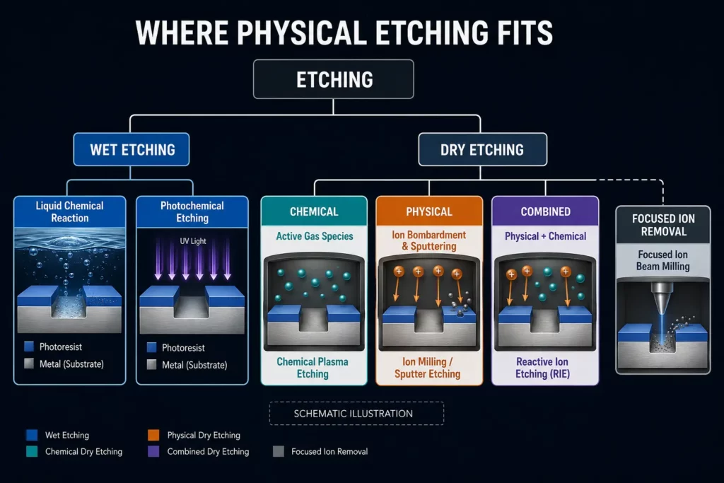
Etching methods can be classified by both the process environment and the removal mechanism.
The two broad process environments are:
- Wet etching
- Dry etching
Wet etching uses liquid chemicals. Dry etching uses gases, ions, plasma or particle beams.
Within dry etching, material can be removed through physical action, chemical reactions or both.
| Etching method | Main removal mechanism | Typical example |
|---|---|---|
| Wet chemical etching | Reaction with a liquid etchant | Photochemical etching |
| Chemical dry etching | Reaction with active gas species | Chemical plasma etching |
| Physical dry etching | Ion bombardment and sputtering | Ion milling |
| Combined dry etching | Ion bombardment plus chemical reaction | Reactive ion etching |
| Focused ion removal | Localized sputtering with a focused beam | Focused ion beam milling |
This classification helps explain why physical etching and plasma etching should not be treated as exact synonyms.
How Does the Physical Etching Process Work?
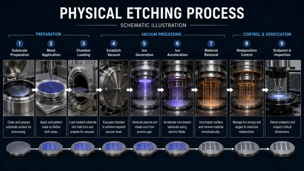
A physical etching system directs energetic ions toward selected areas of a substrate. The process normally takes place in a controlled chamber.
1. Prepare the Substrate
The substrate must be clean enough for masking and controlled processing.
Preparation may include:
- Removing particles
- Removing oil or organic contamination
- Cleaning surface oxides
- Drying the substrate
- Inspecting the starting surface
The preparation method depends on the substrate and final application.
2. Apply the Mask
A mask protects areas that must remain.
Possible masking materials include:
- Photoresist
- Metal masks
- Dielectric masks
- Mechanically positioned masks
- Other process-specific hard masks
The mask must resist ion bombardment long enough to preserve the intended pattern.
Mask selection is important because physical etching may remove the mask and target material at similar rates.
3. Load the Process Chamber
The substrate is placed on a holder inside the chamber.
The holder may support:
- Temperature control
- Rotation
- Tilting
- Electrical bias
- Backside cooling
- Multiple substrate positions
These functions help control uniformity, sidewall angle and heat.
4. Establish the Process Pressure
Air is removed from the chamber to create a vacuum or low-pressure environment.
Low pressure allows the ions to travel toward the substrate with fewer collisions. This supports a more controlled and directional ion beam.
The required pressure depends on the process and equipment.
5. Generate the Ions
A gas enters the system and receives energy from an electrical or radio-frequency source.
The energy ionizes part of the gas. The resulting ions can then be accelerated toward the substrate.
Inert gases such as argon are commonly used for mainly physical removal because they do not need to react chemically with the substrate.
6. Accelerate the Ions
An electric field or ion-source grid accelerates the positive ions.
The ion energy, flux and angle influence:
- Material-removal rate
- Directionality
- Surface damage
- Mask erosion
- Heat generation
- Final surface condition
Increasing ion energy does not always improve the result. Higher energy can increase removal but may also damage the substrate.
7. Remove the Exposed Material
The accelerated ions strike exposed regions of the substrate.
Each impact transfers momentum to atoms in the surface. Some atoms receive enough energy to leave the material.
The process continues until the required depth or layer removal is reached.
8. Control Redeposition
The removed atoms do not always become gases. Some may land on another part of the substrate, mask or chamber.
This effect is called redeposition.
Redeposition can affect:
- Sidewall shape
- Surface roughness
- Feature dimensions
- Electrical performance
- Later cleaning requirements
Chamber pressure, substrate angle, rotation and process geometry can influence where sputtered material travels.
9. Stop and Inspect the Process
The process ends when the target layer or depth has been reached.
Inspection may check:
- Etch depth
- Sidewall profile
- Surface roughness
- Remaining mask
- Redeposition
- Uniformity
- Material damage
Some systems use optical or mass-based monitoring methods to help identify the process endpoint.
Main Types of Physical Etching
Physical etching is not one single process. Several methods use ion bombardment in different ways.
Sputter Etching
Sputter etching uses energetic ions to remove atoms from a surface. The substrate may be electrically biased so that positive ions accelerate toward it.
Argon is often used because it can provide physical bombardment without requiring a strong chemical reaction.
Main Characteristics
- Mainly physical material removal
- Directional ion movement
- Little dependence on chemical reactivity
- Limited material selectivity
- Possible surface and lattice damage
- Possible redeposition
Sputter etching may be used for surface cleaning, oxide removal, pattern transfer and preparation before another vacuum process.
Ion Milling
Ion milling directs a beam of ions toward the substrate. It is also called ion beam milling in many applications.
The ion source is often separate from the main process chamber. This arrangement allows the system to control ion energy, flux and beam direction.
Ion milling is useful when the target material is difficult to remove through a selective chemical reaction.
MKS Instruments describes sputtering and ion milling as physical processes in which positive ions strike a substrate. It also notes their directional behavior, low selectivity and possible surface damage. MKS Instruments
Broad Ion Beam Milling
Broad ion beam milling treats a larger area of a sample.
It can be used for:
- Surface preparation
- Cross-section preparation
- Thin-film removal
- Pattern transfer
- Optical and magnetic components
Focused Ion Beam Milling
Focused ion beam milling directs a very small ion beam toward a selected location.
It is commonly used for:
- Site-specific material removal
- Failure analysis
- Circuit modification
- Cross-section preparation
- Microscopy sample preparation
- Research-scale micro- and nanomachining
Focused ion beam systems provide localized control but are not normally selected for high-volume removal across large surfaces.
Ion Beam Etching
Ion beam etching directs a controlled ion beam at a masked substrate.
The substrate may rotate or tilt during processing. Changing the beam angle can affect sidewall profiles and create angled features.
Oxford Instruments explains that inert ions can be used for physical ion beam etching. Reactive gases can also be added to improve removal rate and material selectivity. Oxford Instruments
Physical Ion Beam Etching
Physical ion beam etching uses mainly inert ions. Material removal depends on sputtering rather than a chemical reaction.
Reactive Ion Beam Etching
Reactive ion beam etching adds chemically active species. The process then includes both physical and chemical effects.
Chemically Assisted Ion Beam Etching
Chemically assisted ion beam etching introduces reactive gases near the substrate. The goal is often to increase the volatility of removed material or improve selectivity.
These reactive variants should not be described as purely physical etching.
Is Reactive Ion Etching a Physical Etching Process?
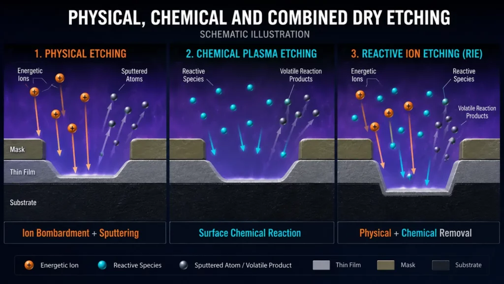
Reactive ion etching, or RIE, is not a purely physical process.
RIE combines:
- Directional ion bombardment
- Reactive gas species
- Surface chemical reactions
- Vacuum removal of volatile by-products
The physical component helps create directionality. The chemical component can improve material selectivity and removal rate.
OSHA classifies RIE as a combination of physical and chemical etching. OSHA
This is an important distinction:
- Ion milling is mainly physical.
- Chemical plasma etching is mainly reactive.
- RIE combines both mechanisms.
For a broader project-level comparison, see Chemical Etching vs Plasma Etching.
What Controls the Physical Etching Result?
Physical etching results depend on several interacting variables.
Ion Species
The ion type affects momentum transfer and sputter yield.
Heavier ions may transfer more momentum, but they may also increase surface damage. Inert ions reduce dependence on chemical reactions but do not guarantee identical removal rates across materials.
Ion Energy
Ion energy influences how strongly the ions strike the surface.
Higher energy may increase material removal. It can also increase:
- Substrate damage
- Heating
- Mask erosion
- Ion implantation
- Surface roughness
The correct energy depends on the target material and acceptable damage level.
Ion Flux
Ion flux describes how many ions reach the surface during a given time.
A higher flux can increase removal rate. However, it may also increase temperature and process instability.
Beam Angle
The angle between the ion beam and the surface affects:
- Sputter yield
- Sidewall angle
- Feature profile
- Redeposition
- Surface uniformity
Some systems rotate or tilt the substrate to improve uniformity or produce a specific profile.
Chamber Pressure
Pressure affects the distance ions can travel before colliding with other particles.
Lower pressure generally supports a more directional beam. Other process requirements may still determine the final pressure range.
Substrate Temperature
Ion bombardment can heat the substrate.
Temperature changes may affect:
- Photoresist stability
- Mask durability
- Material structure
- Surface roughness
- Process repeatability
Cooling or controlled heating may be needed.
Mask Selectivity
Selectivity compares how quickly the target material and mask are removed.
Pure physical sputtering often has lower selectivity than a carefully matched chemical process. The ion beam may attack both materials.
A poor selectivity ratio can cause:
- Premature mask loss
- Dimensional error
- Rounded features
- Surface contamination
- Incomplete pattern transfer
Material Sputter Yield
Sputter yield describes how many surface atoms are removed by the incoming ions.
It depends on:
- Ion mass
- Target atom mass
- Ion energy
- Impact angle
- Surface binding energy
- Material structure
Different materials in the same stack may therefore etch at different rates.

Directionality and Anisotropic Etching
Physical etching is valued for its directionality.
An anisotropic process removes material more strongly in one direction than another. In patterned etching, this often means more downward removal and less sideways removal.
Directional ions can help create:
- Steeper sidewalls
- Narrow trenches
- Controlled edge angles
- High-resolution patterns
- Slanted or shaped profiles
However, physical etching does not automatically produce perfect vertical walls.
The final profile may still be affected by:
- Mask erosion
- Sidewall redeposition
- Beam divergence
- Substrate charging
- Local feature geometry
- Material differences
- Process drift
Directional control is an advantage, not a guarantee.
Materials Used in Physical Etching
Physical etching can remove many solid materials because it does not depend mainly on finding a selective liquid etchant. By comparison, photochemical etching materials must be matched with a suitable etchant and process conditions.
Possible materials include:
- Metals
- Magnetic metal stacks
- Semiconductor materials
- Dielectric films
- Optical materials
- Glass
- Ceramics
- Compound semiconductors
- Superconducting films
- Multilayer thin-film structures
Examples may include gold, platinum, titanium, silicon-based materials and III-V semiconductor materials.
However, “physical etching can remove the material” does not mean it is automatically the best process.
The supplier must also evaluate:
- Sputter yield
- Required depth
- Surface damage limits
- Mask durability
- Redeposition risk
- Required selectivity
- Throughput
- Post-etch cleaning
Oxford Instruments lists metal stacks, dielectric films, photonic materials, magnetic memory structures and superconducting films among ion beam etching applications. Oxford Instruments
Advantages of Physical Etching
Strong Directional Control
Accelerated ions can travel toward the substrate in a controlled direction.
This supports anisotropic removal and more controlled sidewall profiles.
Less Dependence on Material Chemistry
Physical etching does not require the target material to react easily with a liquid or gas-phase etchant.
It can therefore be considered for chemically resistant materials or complex material stacks.
Suitable for Multilayer Structures
A physical process may remove several materials without developing a separate chemical reaction for every layer.
This can be useful when a multilayer structure contains materials with very different chemical properties.
The tradeoff is lower selectivity.
Controlled Beam Angle
Ion beam systems can adjust the substrate or beam angle.
This supports:
- Angled features
- Sidewall shaping
- Surface smoothing
- Profile correction
- Specialized optical structures
No Liquid Etchant During Material Removal
The physical removal stage does not require a liquid etchant bath.
Other wet cleaning, masking or development steps may still be part of the complete manufacturing process.
Integration With Vacuum Processing
Physical etching can be integrated with other vacuum-based processes, such as:
- Thin-film deposition
- Surface analysis
- Plasma cleaning
- Optical coating
- Semiconductor processing
This may reduce exposure to the external environment between process steps.
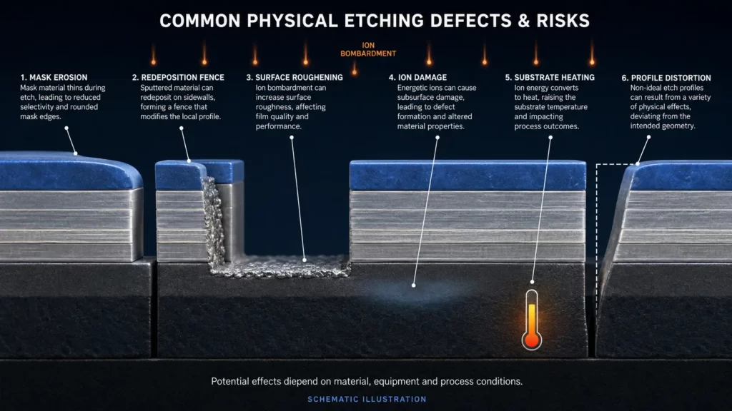
Limitations of Physical Etching
Physical etching is useful, but it also has important limits.
Low Material Selectivity
Physical ion bombardment may remove the target material, mask and neighboring layers.
This makes it harder to stop precisely on another material.
Reactive chemistry can improve selectivity, but the process is no longer purely physical.
Slow Material-Removal Rate
Pure physical sputtering can be slower than chemical or reactive etching. Chemical processes have different constraints, including material thickness, undercut and minimum feature size, as explained in the limitations of photochemical etching.
The process becomes less practical as the required removal depth or treated area increases.
Physical etching is normally better suited to thin layers and specialized structures than thick bulk material.
Surface and Subsurface Damage
Energetic ions can affect more than the atoms that leave the surface.
Possible effects include:
- Lattice damage
- Amorphization
- Ion implantation
- Defect formation
- Electrical property changes
- Optical property changes
- Roughness changes
Damage sensitivity must be considered for semiconductor, optical and functional materials.
Redeposition
Removed atoms may settle on another part of the feature.
Redeposition can create:
- Sidewall deposits
- Fences around patterns
- Contamination
- Electrical shorts
- Rough surfaces
- Difficult post-etch cleaning
The risk depends on process geometry, chamber conditions and material volatility.
Mask Erosion
The ion beam can remove the masking material.
If the mask erodes too quickly, the final feature may become wider, rounded or incomplete.
A thicker or more resistant mask may be necessary.
Substrate Heating
Ion impacts add energy to the substrate.
Excess heat may damage:
- Photoresist
- Polymer layers
- Adhesive layers
- Temperature-sensitive films
- Delicate multilayer structures
Temperature monitoring and cooling may be required.
Surface Roughening
Physical etching may roughen some materials instead of producing a smooth surface.
The result depends on:
- Material grain structure
- Ion energy
- Beam angle
- Initial surface condition
- Process time
- Preferential sputtering
A process developed for one material should not be assumed to produce the same finish on another.
High Equipment Cost
Physical etching normally requires:
- Vacuum equipment
- Ion or plasma sources
- Power supplies
- Gas delivery
- Substrate cooling
- Exhaust handling
- Process monitoring
- Chamber maintenance
The equipment and operation are more complex than a simple liquid etching bath.
Limited Throughput for Bulk Removal
Ion beams remove material from surfaces or thin layers.
They are generally not the best choice for manufacturing thick sheet metal parts, deep bulk cavities or large quantities of conventional components.
Common Applications of Physical Etching
Semiconductor Patterning
Physical etching can remove selected semiconductor, metal or dielectric layers.
It may be used when strong directionality is needed or when the material does not respond well to available chemical processes.
Magnetic Memory Devices
Ion beam etching is used for some magnetoresistive random-access memory structures.
These devices can contain multilayer magnetic and metal stacks that are difficult to process with one selective chemistry.
Optical and Photonic Components
Directional ion beams can form:
- Laser facets
- Waveguide features
- Slanted structures
- Optical gratings
- Photonic device patterns
Beam angle control can be important for these applications.
Thin-Film Patterning
Physical etching can remove selected thin-film areas after masking.
Applications include:
- Metal tracks
- Contact structures
- Dielectric films
- Optical coatings
- Research devices
Surface Cleaning
Low-level sputtering can remove:
- Native oxides
- Organic contamination
- Surface residues
- Weakly bonded layers
This can prepare a surface for deposition, analysis or bonding.
Over-processing can damage or roughen the surface.
Materials Analysis
Ion milling is often used to prepare samples for:
- Electron microscopy
- Cross-section inspection
- Failure analysis
- Thin-film analysis
- Surface and depth profiling
The process can reveal buried layers or prepare a more suitable inspection surface.
Micro- and Nanomachining
Focused ion beams can remove material from selected locations.
This supports:
- Circuit repair
- Local cross-sectioning
- Device modification
- Prototype research
- Site-specific sample preparation
This use is highly precise but normally has low throughput.
Physical Etching vs Chemical Etching
Physical and chemical etching remove material through different mechanisms.
| Factor | Physical etching | Chemical etching |
|---|---|---|
| Main mechanism | Ion bombardment and sputtering | Chemical reaction |
| Typical environment | Vacuum or low-pressure chamber | Liquid etching system |
| Common workpiece | Wafers, thin films and substrates | Metal sheet and foil |
| Directionality | Often strongly directional | Often more isotropic |
| Material selectivity | Often limited | Can be high with suitable chemistry |
| Surface damage | Possible ion damage | No energetic ion bombardment |
| Main tooling | Mask and chamber process | Digital artwork and photo tooling |
| Typical depth | Surface layers and thin films | Through-features in thin metal |
| Main applications | Semiconductor, optics, MEMS and analysis | Precision flat metal components |
| Main limitation | Damage, redeposition and equipment cost | Undercut and thickness-related limits |
Chemical etching is usually more suitable when the required output is a separate thin metal part. Physical etching is more suitable when the target is a film, wafer surface or specialized microstructure.
Learn more about the chemical etching process and its use in precision metal manufacturing.
When Is Physical Etching the Right Process?
Physical etching may be a good choice when:
- The target is a thin film or surface layer.
- The substrate must remain part of the final device.
- Directional removal is important.
- The material is difficult to remove chemically.
- The design includes a complex multilayer stack.
- Controlled sidewall angles are required.
- The process must integrate with other vacuum stages.
- The application is semiconductor, optical, magnetic or research-based.
- Surface preparation is required before deposition or analysis.
A process specialist should review the full material stack, not only the top layer.
When Is Physical Etching Not the Best Choice?
Consider another process when:
- The project requires complete parts from metal sheet.
- The required removal depth is large.
- Production volume requires rapid bulk material removal.
- The substrate is highly sensitive to ion damage.
- Strong selectivity between layers is essential.
- Redeposition could create unacceptable defects.
- The mask cannot survive the required process time.
- Vacuum processing adds unnecessary cost.
- The design contains conventional sheet metal profiles and through-holes.
For thin, flat precision metal parts, photochemical etching may provide a more practical route.
Information Needed Before Selecting Physical Etching
Provide the following information to the process supplier:
- Complete material stack
- Target material
- Underlying materials
- Mask material
- Layer thickness
- Required removal depth
- Smallest feature
- Sidewall angle
- Surface roughness limit
- Damage sensitivity
- Electrical or optical requirements
- Acceptable redeposition
- Temperature limit
- Sample or wafer size
- Required production quantity
- Inspection method
- Upstream and downstream processes
The supplier may need test samples before confirming the final recipe.
Frequently Asked Questions
Is Physical Etching the Same as Plasma Etching?
No.
Physical etching describes a material-removal mechanism based on ion bombardment. Plasma etching describes a broader process category that may use physical action, chemical reactions or both.
Is Ion Milling a Physical Etching Process?
Yes. Ion milling normally removes material through sputtering caused by energetic ions.
Reactive gases may be added in some ion beam systems. In that case, the process includes a chemical component.
Is Sputter Etching the Same as Ion Milling?
The terms are closely related, but equipment arrangements may differ.
Both use energetic ions to eject atoms. Ion milling often uses a separate ion source to create a controlled beam, while sputter etching may accelerate ions directly toward a biased substrate.
Does Physical Etching Use Chemicals?
Pure physical etching mainly uses inert ions rather than a chemical reaction.
However, the complete process may still use gases, photoresist, developers, cleaning chemicals or reactive additives.
Can Physical Etching Remove Any Material?
Physical bombardment can remove many materials, including materials that are hard to process chemically.
Removal rate, damage, mask selectivity and surface quality still vary by material. Technical capability does not always mean commercial suitability.
Does Physical Etching Eliminate Undercut?
Physical etching can reduce lateral removal because the ions are directional.
It does not automatically eliminate mask erosion, sidewall variation, beam divergence or redeposition.
Is Physical Etching Faster Than Chemical Etching?
Not usually for bulk material removal.
Pure physical sputtering can have a lower removal rate than chemical or reactive processes. Speed depends on the material, depth, treated area, ion energy and equipment.
Is Physical Etching Suitable for Thick Metal Parts?
Physical etching is generally not the first choice for thick metal parts.
It is mainly used for surface layers, thin films and specialized structures. CNC machining, laser cutting, waterjet cutting or another process may be more suitable for thick material.
Which Is More Precise: Physical or Chemical Etching?
Precision depends on what must be manufactured.
Physical etching can provide directional control for small thin-film structures. Chemical etching tolerances for thin sheet metal parts depend on material, thickness and feature geometry. Their capabilities should not be compared without defining the material, scale and geometry.
Conclusion
Physical etching removes material through the impact of energetic ions. Sputter etching, ion milling and inert ion beam etching are common examples.
Its main advantages are directional removal, controlled beam angles and reduced dependence on chemical reactivity. These characteristics make it useful for semiconductor, optical, magnetic and thin-film applications.
Its main limitations include low selectivity, slow bulk removal, mask erosion, redeposition, surface damage and high equipment complexity.
Physical etching is not simply another name for plasma etching. Some plasma processes are mainly chemical, some are mainly physical and processes such as RIE combine both mechanisms.
If your project involves a wafer, thin film or microfabricated structure, consult a qualified physical or plasma etching specialist. If you need a complete precision component made from metal sheet or foil, contact TMNetch for a photochemical etching feasibility review.