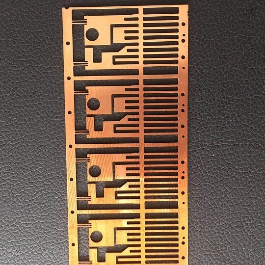
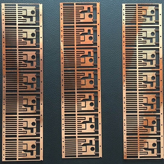
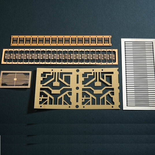
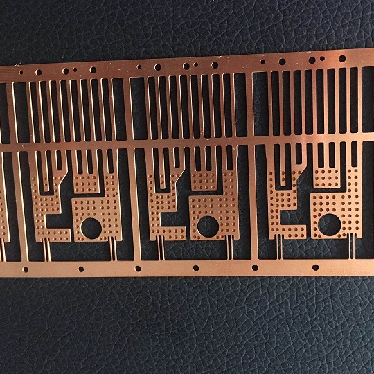
Custom IC lead frame
1. What’s the production capacity of TMN for Lead Frame Parts?
TMN has more than 10 years experience of OEM & ODM the shielding parts with 4000 square meters workshop and 100 experienced workers and engineers
5 automatic etching production lines with 20 meters long.
2 automatic cleaning equipment, 6 stamping machines.
The production capacity of TMN is 300000pcs.
Enough experience of export shielding parts to the USA, UK, Canada, Korea, Germany, Netherlands, Singapore, Russia, Iran, Israel, Austria, Australia and so on.
Designed all Lead Frames for different industries, such as Aerospace, Automotive, Industrial, Marine, Medical, Military, Electronic, etc.
2. What are the main raw materials of Lead Frame covers and clips?
Stainless Steel Alloys, Copper Alloys, Brass Alloys, Aluminum Alloys, Nickel Silver, Some other special requested metal materials.
3. What’s the thickness of the raw materials and the tolerance can be reached by photochemical etching?
· Thickness: 0.001 inch to 0.078 inch
· Tolerance : +/- 0.001inch
4. What’s the process for coating/plating after photo etching can be done?
· Nickel plating 1~10μ
· Tin plating 1~10μ
· Ag plating 1~10μ
· Au plating 1~10μ
5. What are the advantages of TMN manufacturing plants?
· Rapid for prototypes without any tools (1~3 days can be finished the prototypes)
· No scratches and no burrs
· Designs can be changed flexibly
· High precision with a small tolerance
6. What’s the lead time for samples, and how many samples can be provided for the first time?
· 10PCS samples can be provided for confirmation and 4 days as the lead time for common materials, if the raw material is special, it will take some days to prepare raw materials.
· For mass production, it is about 10 days after confirming all details.
More about Lead Frames
In the world of semiconductor production lead frames have a critically important role as they are the base for numerous electronic instruments. It means that these complex forms are essential for such purposes as creating electrical circuits; strengthening construction; and attaining thrombotic characteristics.
In this convoluted landscape of making semiconductors, these frames are a necessity. These complex designs are a critical component of numerous electronics devices as they are used to create path ways for electrical signals, give structural support for mechanical interfaces and aid in thermal management. Lead frames provide an accurate and efficient structure and fabrication for circuits, miniature lighting or semiconducting sensing components, that underpin the current digital environment. Take a deep look into the heart of semiconductor innovation and understand the role of lead frames to drive our electronics today.
How to Contact TMN?
TMN's lead frame solutions are perfect for the fast-moving electronics industry. They provide a cost-effective and efficient way to make precise lead frames needed for super-small connections and lots of pins. Our method beats traditional stamping hands down!
If you want to inquiry TMN, just need to send an email to lydia.sales1@tmnetch.comwith drawings at the format of DXF, DWG, PDF, 7*24 hours available.
Our Team And Factory


